feedback reduces distortion porportional to excess loop gain - you should want the highest open loop gain as long as the open loop dstortion porportional increase isn't more than the porportional gain increase - you "win" on stage distortion after feedback
the "beta enhancement" buffer ef between diff pair and VAS Q is a huge win since it adds very little distortion for a huge increase in open loop gain (with mirror loaded diff pair)
likewise increasing load Z ("triple" or mosfet output) gives large dividends in increased VAS gain
we could look at the # but I'd guess Vbe modulation cancellation, cascode (without load Z increasing measures) are a relative sideshow compared to these major loop gain boosts
Last edited:
That's not surprising (about the cancellation) as it's quite possible for capacitances that vary with voltage to have a cancellation effect, similarly conductances.
For fun I just simmed a couple of the simplest bipolar common-emitter amps with a simplest-JFET-I source as load versus a perfect current source. The JFET source had about 20dB lower distortion, mostly due to a reduction in second. This was with very small signal voltages at the base, and adjusted to give equal output swings at the collector.
For fun I just simmed a couple of the simplest bipolar common-emitter amps with a simplest-JFET-I source as load versus a perfect current source. The JFET source had about 20dB lower distortion, mostly due to a reduction in second. This was with very small signal voltages at the base, and adjusted to give equal output swings at the collector.
Another way to look at the CCS issue: Drive it with a current source excitation and look at the distortion at the junction. Some resistive loading connected to some voltage reference will be needed for the higher-impedance CCS circuits, as otherwise it will be impossible to stabilize and the gain will be insanely high.
One should see a complementing distortion, and that can be a guide as to what compensation with a voltage amplifier might require.
The secret sauce with the gain stage posted a bit back in this thread is that the two base-emitter voltages have compensating nonlinearities when driven with approximately equal currents.
Some examples of compensatory nonlinearities
Here are five cases of completely impractical circuits that show the effects of various means of sourcing current.
Impractical, but instructive. The transistor is being driven from an ideal voltage source. The collector output is being measured with an infinite-impedance probe. There is no accounting for temperature variations with signal or ambient.
In succession, from left to right and top to bottom, we have a resistive load, an ideal current source load, a simple JFET current source load, a bipolar complement to the BD139 set up to provide the current (~a BD140), and finally a stage in which both the NPN and the PNP are driven, with the levels adjusted to approximately minimize distortion. I've arranged them in order of decreasing total (to 14th harmonic) distortion, but included the individual contributions at each harmonic below each circuit.
Note that the drive signal for each circuit is adjusted to provide about the same output voltage at the collector(s). Each d.c. output voltage is about zero. The gains are significantly different, with as expected the ideal I source load having the highest gain, the resistive load the lowest.
Attachments
Regarding function of R1 "magic" & clipping control
Just reading through this thread so I refer here back a couple of months
Are you assuming imperfect CCS operation for R1 to have any effect as "magic" resistor ? presumably the higher impedance the CCS the less effect R1 can have . . . or is it called "magic" because any effect would seem impossible ?
I guess it does, but that wasn't a design consideration. I expect that allowing voltage swing on Q1's collector actually makes distortion a bit worse, especially as Vce is so low to start with. I considered that a small price to pay in exchange for civilized clipping behavior though.
Just reading through this thread so I refer here back a couple of months
Are you assuming imperfect CCS operation for R1 to have any effect as "magic" resistor ? presumably the higher impedance the CCS the less effect R1 can have . . . or is it called "magic" because any effect would seem impossible ?
No magic.Are you assuming imperfect CCS operation for R1 to have any effect as "magic" resistor ?
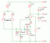
Those comments were referring to the circuit below. R1, D1 and D3 are for current limiting. Someone else asked if R1 was a "magic" resistor (to reduce thermal distortion), but that's not why it's there.
Maybe you thought the comments were referring to R1 in the other circuit?
Attachments
This one has about 44dB of gain. Max output is about 14Vrms @ 0.08% distortion. Bandwidth is good with no peaks. Maybe not enough voltage for a high power amp, but I think it's pretty good. I like the SRPP. Also, they can be optimized for load impedance. I changed the load resistor to get a low distortion value. It's funny but the distortion goes up when the load is too and when the load is too high.
Attachments
14Vac of maximum output from a +-24Vdc supply is pretty good.
Why do you think otherwise?
Oh, I don't know, maybe just from lack of experience in designing high power amps (like none at all). I've fooled around with designs for lower power (50 watts or so) amps.
That's a really good article. I like Broskie's stuff, and his analogies are great fun.
Thx - not a million miles from a JLH simple class A o/p stage - which is also a VAS
( and also in a description defying no man's land between SE & PP )
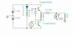
Well, I got to thinking and fooling around. Two power transistors in SRPP formation. One watt into 8 ohms with about 1.5% distortion. Not terrible, but not outstanding either. Given that at the time there weren't any good complementary transistors, I guess this was not too shabby.
Attachments
I'm looking for a VAS topology that has really good PSRR.
Me too.
Have a look at Samuel Groner's comments on Self's Book, fig. 56 p 48.The SRPP I've been playing with is not very good at all. The bias network is a big problem for one thing. Does anyone have a VAS that has really good PSRR?
I made a PCB but currently it's only work in progress.
Check out my post #32 and #44I'm looking for a VAS topology that has really good PSRR. The SRPP I've been playing with is not very good at all. The bias network is a big problem for one thing. Does anyone have a VAS that has really good PSRR?
Me too.
Have a look at Samuel Groner's comments on Self's Book, fig. 56 p 48.
I made a PCB but currently it's only work in progress.
OK, I was thinking about a differential VAS. Thanks.
- Status
- This old topic is closed. If you want to reopen this topic, contact a moderator using the "Report Post" button.
- Home
- Amplifiers
- Solid State
- Best VAS?