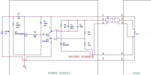
Wiring
This is how I'm wiring this regulator. If the regulator is in the same case with the phono stage you may delete 3 and the shielded cable T1, and simply star the output/sense and the grounds/sense at the low noise input stage terminals.
I guarantee that using this schema will improve the performance. Can't say about the sound, but if there's any impact it will definitely be larger than the effect of an overnight burn-in. Also, if the MOSFET you are using hass Ciss lower than the NTP in my schematic, you may want to proportionally increas the gate resistor, to keep the pole unchanged.
Attachments
Syn,
why have you duplicated the route 3 and route 4 to the load sense point?
This is one of the very rare occasions where the designer has properly drawn the schematic to show how to implement connections/traces that ensure the design works as intended.
I do wish all designers would do this.
Uchi's extra resistor should be 125r to match impedances at the two opamp inputs.
But, this value only applies if the effective impedance of the LED ref is zero.
Any idea what the LED ref impedance is?
AndrewT said:Syn,
why have you duplicated the route 3 and route 4 to the load sense point?
This is one of the very rare occasions where the designer has properly drawn the schematic to show how to implement connections/traces that ensure the design works as intended.
I do wish all designers would do this.
Uchi's extra resistor should be 125r to match impedances at the two opamp inputs.
But, this value only applies if the effective impedance of the LED ref is zero.
Any idea what the LED ref impedance is?
Because you don't want any DC trough the shielding. 4-4 should have a lower impedance, so current goes through there. Another idea is to leave the right 3 open, but I usually prefer to connect both ends.
If possible, I would avoid the 125 ohm resistor. It adds noise to the output.
You are correct, e.g. without proper wiring something like the PGP amp would never be possible. See the wiring schematic on my web site http://www.synaesthesia.ca/Wiring.html
Edit: As it is, the output voltage is about 30V and of course, the raw power supply has to provide at least about 35V. You may want to adjust the R3/R4 divider for other values.
When I've used LEDs for voltage reference purposes (at 1-3mA) I've seen impedances c.35-50ohms. Pretty low actually, and significantly better than a zener at these currentsAny idea what the LED ref impedance is?
hi syn08
After examining your circuit again i have to admit i don't quite understand it and will appreciate some hints.
1. Why bypassing R5 important for the high frequency performance? Is R5 not there simply to supply current for the voltage source? And presumably can be replaced with a ccs for better performance?
2. Why is the connection from R5 taken to the sense point? I understand the connection to R4 but again, is R5 not simply supplying stable current to the led?
3. I would probably not ask 1 and 2 if i could get the circuit to work as shown, but i can't. As soon as there is a cap above 100n across R5 i get low-frequency oscillations seemingly determined by the LED impedance and the cap.
I don't know how important any of this is. Fed from a ccs instead of a resistor this shunt sounds quite spectacular.
analog_sa said:hi syn08
After examining your circuit again i have to admit i don't quite understand it and will appreciate some hints.
1. Why bypassing R5 important for the high frequency performance? Is R5 not there simply to supply current for the voltage source? And presumably can be replaced with a ccs for better performance?
2. Why is the connection from R5 taken to the sense point? I understand the connection to R4 but again, is R5 not simply supplying stable current to the led?
3. I would probably not ask 1 and 2 if i could get the circuit to work as shown, but i can't. As soon as there is a cap above 100n across R5 i get low-frequency oscillations seemingly determined by the LED impedance and the cap.
I don't know how important any of this is. Fed from a ccs instead of a resistor this shunt sounds quite spectacular.
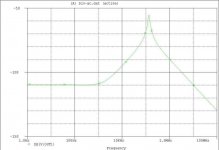
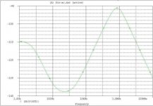
1. If you think in terms of sound, I have no explanation. Otherwise, the output impedance and the line regulation are both much, much better with R5 bypassed. Think of the caps as being included in the loop and the opamp acting as a capacitor multiplier. See the next two messages for results.
2. For the same reason as above. See also the Jung regulator articles, they use the same schema for connecting the reference current source.
3. I'm pretty sure you have grounding issues. From my experience, it is also unlikely you'll ever have good performance for this regulator built on a breadboard. Try point to point with short connections.
analog_sa said:Line regulation is something i largely don't care about. Plus i have preregulators. Do you have similar pictures for noise?
No, but obviously if the output impedance is minimized up to RF, so will the output noise.
One thing I can't explain is the positive impact of the CCS instead of the balast resistor. I can't measure any difference up to 10MHz in line regulation, output impedance and noise.
But then, whatever pleases your ear
") This solution is (to me) much simpler than the Jung regulator and is ideal for class A gain stages (where the power dissipation of the parallel regulator can be minimized).
This solution is (to me) much simpler than the Jung regulator and is ideal for class A gain stages (where the power dissipation of the parallel regulator can be minimized).Glad you like it
janneman said:Hi Syn08,
Have you considered to use a couple of LEDs or a low-noise ref chip to increase the reference? That would increase your loop gain for possibly even better performance. No criticism, just curiosity.
BTW Your remote sensing is right on target
Jan Didden
I've tried:
- LM329 (6.9V) is worse in tems of noise, plus limited bandwidth (up to 500KHz)
- TL431 has very poor noise and limited bandwidth, plus the well known stability issues. I was unable to keep the output impedance low, over 150KHz
Haven't tried multiple LEDs, but it's worth of. I'm though expecting some noise degradation. What I can tell is that only infrared or red LEDs should be used. Anything else (and in particular blue and violet, tempting because they have Vf=3.5-4V) have way to much noise.
syn08 said:
I've tried:
- LM329 (6.9V) is worse in tems of noise, plus limited bandwidth (up to 500KHz)
- TL431 has very poor noise and limited bandwidth, plus the well known stability issues. I was unable to keep the output impedance low, over 150KHz
Haven't tried multiple LEDs, but it's worth of. I'm though expecting some noise degradation. What I can tell is that only infrared or red LEDs should be used. Anything else (and in particular blue and violet, tempting because they have Vf=3.5-4V) have way to much noise.
Right. I think there are some modern low-noise references around these days, need to look it up. But gain may be small anyway.
Jan Didden
janneman said:
Right. I think there are some modern low-noise references around these days, need to look it up. But gain may be small anyway.
Jan Didden
The only thing that I found better in terms of noise was a MAX6126AASA25 2.5V reference. Frequency response was acceptable (up to 500KHz) but unfortunately this IC has a very ugly line and load transient response. And unfortunately it takes only 12V input, so I haven't looked closer...
And of course, at $17 a pop...
I’m sorry, I can’t see the regulator in post 21’s schematic working at all. The gain of the error amp is set by the feedback loop ratio of R4 & 5, which as pictured is around 26. The LED reference should be around a volt or so for that LED (looking at the data sheet), so that would yield an output voltage of around 26V. The input is only 15 volts in the schematic. What’s the output voltage supposed to be?? The addition of C1 & 2 across R5 is a positive feedback path and should lead to worse noise, if not outright instability. Perhaps C3 mitigates that to some degree (lag vs. lead)?? Sounds tricky at best. Commonly, despite the pictures, C1 & 2 would be across D1 (C1 would be made somewhat larger in that case), with a counter diode across R5 to protect U13’s input from the charge stored in C1 & 2 at power down. To reduce noise it’s common to place a cap across the feedback resistor, in this case R4, though stability issues need to be considered when that’s done. I’m at a loss as to how this regulator can be expected to work optimally as pictured. Am I missing something?? Sorry, don’t mean to come across harsh, just at a loss …
syn08 said:
The only thing that I found better in terms of noise was a MAX6126AASA25 2.5V reference. Frequency response was acceptable (up to 500KHz) but unfortunately this IC has a very ugly line and load transient response. And unfortunately it takes only 12V input, so I haven't looked closer...
And of course, at $17 a pop...
How about LT1027?
kaos said:Am I missing something??
As i mentioned earlier on i recalculated resistor values which work. The rest of your post makes perfectly good sense to me as well.
kaos said:I’m sorry, I can’t see the regulator in post 21’s schematic working at all. The gain of the error amp is set by the feedback loop ratio of R4 & 5, which as pictured is around 26. The LED reference should be around a volt or so for that LED (looking at the data sheet), so that would yield an output voltage of around 26V. The input is only 15 volts in the schematic. What’s the output voltage supposed to be?? The addition of C1 & 2 across R5 is a positive feedback path and should lead to worse noise, if not outright instability. Perhaps C3 mitigates that to some degree (lag vs. lead)?? Sounds tricky at best. Commonly, despite the pictures, C1 & 2 would be across D1 (C1 would be made somewhat larger in that case), with a counter diode across R5 to protect U13’s input from the charge stored in C1 & 2 at power down. To reduce noise it’s common to place a cap across the feedback resistor, in this case R4, though stability issues need to be considered when that’s done. I’m at a loss as to how this regulator can be expected to work optimally as pictured. Am I missing something?? Sorry, don’t mean to come across harsh, just at a loss …
The error amp works open loop. The opamp compares the ref with 1/26 of the output, and any error is amplified by the open loop gain and drives the MOSFET to bring the error back to (close to) zero. Works like a charm.
Edit: My comment about using a higher ref voltage means that you can make the 1/26 ratio bigger so that the loop gain increases and the error decreases.
Jan Didden
kaos said:Am I missing something??
Yes. You miss the understanding on how parallel regulators are working
Sorry, don’t mean to come across harsh, etc...- Status
- This old topic is closed. If you want to reopen this topic, contact a moderator using the "Report Post" button.
- Home
- Amplifiers
- Power Supplies
- Best low noise regulator?