What current draw do you get on lower device with 4V7?
Runaway at above 8A. It picked up speed as it climbed. past 30V @ 8A = 240W and showed no sign of stopping. So it cut itself off at 8A05 at the limit I set. Please see post #595.
Last edited:
@ C11
This two resistors are soldered at some point or only have contact with crocodile ?
Crocodile. I pull on all connections and this is tight. I had 2 on at first then pull the second one as the first was holding them tight. I confirmed it with DMM too.
Runaway at above 8A. It picked up speed as it climbed. past 30V @ 8A = 240W and showed no sign of stopping. So it cut itself off at 8A05 at the limit I set. Please see post #595.
Is this with top half unpowered as ZM suggested?
Drop to 4V1, then what do you get?
Last edited:
Just to be sure it was not the lower device. I replaced it and rewired back to the schematic except I bypassed the CCS altogether. My bench supply is supplying 28V directly to the drain of the output device as the schematic calls for in the lower half, and with bias av 4V75, the DC offset is at or under 3mV, temp is around 125°F or 52°C.
Lo and behold, after letting it settle, it is drawing 28V at 2A3 for now, let's see how long that holds!
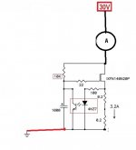
Left pic - no output regardless of bias voltage.
Right pic - I can try that again with the new lower device installed.
But everything happens tomorrow after work now - closing down for tonight!
Thank you all!
Lo and behold, after letting it settle, it is drawing 28V at 2A3 for now, let's see how long that holds!
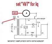
left pic in #591 - can you set 3A2 varying bias (so called 4V7 ) voltage with pot ?
right pic - try another optocoupler if you're getting much more than 3A2
besides that - relocate gate resistors ditto on mosfet gate screw ; at least I can't see them there
Left pic - no output regardless of bias voltage.
Right pic - I can try that again with the new lower device installed.
But everything happens tomorrow after work now - closing down for tonight!
Thank you all!
well , maybe it's a fact that English is not my native language ...... but at least I can't follow you there ;
what offset you're mentioning , when simple current tests are in question?
again - brake circuit in two halves , test exactly per this two schematics , put A -meter where appropriate , and put gate resistors ditto at mosfets if you already didn't
what offset you're mentioning , when simple current tests are in question?
again - brake circuit in two halves , test exactly per this two schematics , put A -meter where appropriate , and put gate resistors ditto at mosfets if you already didn't
Attachments
well , maybe it's a fact that English is not my native language ...... but at least I can't follow you there ;
what offset you're mentioning , when simple current tests are in question?
again - brake circuit in two halves , test exactly per this two schematics , put A -meter where appropriate , and put gate resistors ditto at mosfets if you already didn't
ZM,
I did these test already and the answers are in Post #598. There are pictures too. Here it is again:
"On first picture - left - 0.01A or negligible draw.
Wiring picture shows picture 2 on the right. 5A53 draw and STEADY. This turns on the upper device and it stabilized at about 175°. No runaway. Lower device is cool. The devices are arranged on the heatsink like the schematic - upper is the bias regulator and the lower is the output."
What I have not done is to move the gatestoppers to the screw. I did that earlier but it did not make the runaway stop so I move them back for the time being. Certainly would do that once the layout is finalized.
well , me too.
once there is no current , second time I understand it is , what is offset mentioned etc.
it can't be so hard ......
whatever - common thing for both tests is bench supply ....... besides that , I'm not doubting neither Papa's brain nor physics in schematic ...... so - it must work as intended
once there is no current , second time I understand it is , what is offset mentioned etc.
it can't be so hard ......
whatever - common thing for both tests is bench supply ....... besides that , I'm not doubting neither Papa's brain nor physics in schematic ...... so - it must work as intended
So lower device wasn't working but has been replaced and is working now?
Is that right?
I'm struggling to follow what you've done.
well , me too.
once there is no current , second time I understand it is , what is offset mentioned etc.
it can't be so hard ......
whatever - common thing for both tests is bench supply ....... besides that , I'm not doubting neither Papa's brain nor physics in schematic ...... so - it must work as intended
Gentlemen,
I followed Papa's video thoroughly many times, laid out the schematic for point-to-point wiring, and asked a number of questions in posts on this thread about capacitance, power supply choice etc. Many including 2pD helped with looking over finding misses and mistakes, and Papa responded also several times and I took his advice faithfully. After a few weeks waiting for all parts to arrive, I finally started to put it together and shared what I did step by step in posts - not telling others how to do it, but seeking advice for how to do it right or better.
The core schematic is 100% Papa's, and I believe in his work and physics also. If I did not, I would not started to build it. Aside from one wiring error that was caught early on, it has been triple checked to reflect the published schematic correctly. But I did encounter these problems so I posted and asked for help. Despite this, So far, I found 2 major issues:
1. It appears there is a current draw runaway problem with the output device. With the bias at 4V7 - whether it is coming from the bench supply or a 9V battery through a trimpot - It keeps pushing well past 60V and 3A2. If I did not set a current limit on the 60V bench supplies. it would go straight through to 8A which I saw it do once when checking if it would.
2. It appears also that there is motor-boating, especially when the input is shorted to ground, as when I tried to adjust the bias to minimize DC offset.
There problems were posted, and pictures of the voltage and current draw shown in pictures posted here. implemented every suggestion made to me by 2pD, ZM, Generg - short of building a cap bank PSU. My opinion is that the way the circuit is right now, connecting a cap bank PSU would only trip the circuit breaker when the output device hits the breaker limit since the problem is still with me no matter which suggestion I tried. My comment about the output (lower device) being possibly fixed is because by deduction, the only thing I had not tried was to replace it. I did, but as opposed to driving it with the CCS, I drove it with my 2 bench supplies, delivery 4V75 for bias, and 30V 2A4 for rail. It appeared stable for the 30 minutes I watched it, but the current was still climbing, although very slowly. In other words, it was not rock steady. The comment about DC offset was just one of the checks I also did while watching its stability.
So where do I go from here?
2pD had commented several times that the Vgs for this device is very critical due to its high transconductance. I see this first hand. His circuit from a few weeks back had a LT1431 in it for regulating the bias supply which I now know is pretty much necessary unless there is another way to tame this beast better as the 9V1 Zener in Papa's design may not hold enough sway. Then there is the question of whether the 4N37 is working as it should. I bought 4 Vishay's and am on the second one. Either I am unlucky or there is a better choice. But perhaps they need to be toleranced and sorted just like output devices. Zm just mentioned this now and I may have to start on it.
When these 2 issues are put to bed, then we can discuss how it sounds. I am still optimistic but sometimes i can use some luck too, like getting parts that are in spec, solder properly and don't fry, etc.. So far, it has been elusive. Hope this explains everything in one place.
The 4V7 is not set in stone.
It's meant to be adjusted to get the 28V figure mentioned in the schematic.
It can often takes 30 to 40 minutes before the bias stops climbing. As long as it doesn't jump to over 4A then that is fairly normal.
With the new output device, I got 28V at 2A4, using 4V75. But this was accomplished using my bench supplies both on the rail and bias, NOT the CCS. Even then, the 2A4 appears to continue drifting up over 30 minutes, and is not rock steady, at which point I stopped and went onto to do other things.
So theoretically, I can drive the amp with my bench supplies more than with the CCS if the 4N37 has huge variability that requires meticulously balancing the constellation of parts around it.
Last edited:
1. test for lower half :
to repeat (both my self and pico)ignore 4V7 as value , take it as figure ; set 3A2 in temp equilibrium , even if that demands 2 hours of operation
2. test for upper half - add 10K trimpot in series with red squared 10K resistor (preset to max value); fiddling with that pot , set 3A2 in temp equilibrium , even if that demands 2 hours of operation
3. then only you can connect two halves
On first picture - left - 0.01A or negligible draw.
Wiring picture shows picture 2 on the right. 5A53 draw and STEADY. This turns on the upper device and it stabilized at about 175°. No runaway. Lower device is cool. The devices are arranged on the heatsink like the schematic - upper is the bias regulator and the lower is the output.
Are your both MOSFETs insulated from the heatsink? If not they should be and heatsink should be grounded.
Attachments
Are your both MOSFETs insulated from the heatsink? If not they should be and heatsink should be grounded.
SOT-227 modules are distinguished by these key features:
• Fully isolated from the metal base, allowing common heatsink and compact assemblies to be built
only thermal compound necessary.
http://www.ixys.net/Documents/AppNotes/IXAN0073.pdf
Gentlemen,
Many thanks for your helpful and insightful replies. I will follow ZM's test procedure when I can start again, hopefully in the next few days - going to work now!
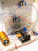
kacernator and generg - thank you both also, you can see the Sil-pads right at the foot of the Jensen ready to go on next ;-)
Thanks to everyone again and I will report back as soon as I can.
Many thanks for your helpful and insightful replies. I will follow ZM's test procedure when I can start again, hopefully in the next few days - going to work now!
kacernator and generg - thank you both also, you can see the Sil-pads right at the foot of the Jensen ready to go on next ;-)
Thanks to everyone again and I will report back as soon as I can.

- Status
- This old topic is closed. If you want to reopen this topic, contact a moderator using the "Report Post" button.
- Home
- Amplifiers
- Pass Labs
- BAF 2015 Coverage