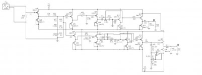
if offset is negative , put 50R-100R trimmer (connected as variable resistor) in source of Q22
if offset is positive , put 50R-100R trimmer (connected as variable resistor ) in source of Q21
or just make correction of offset at output of stage , putting 50R-100R trimmer between S of Q46 and D of Q45 , with wiper as out node
if offset is positive , put 50R-100R trimmer (connected as variable resistor ) in source of Q21
or just make correction of offset at output of stage , putting 50R-100R trimmer between S of Q46 and D of Q45 , with wiper as out node
Last edited:
Thanks ZM, I have thought about this as a a last resort, and actually have trimmers in that range at hands. But what puzzles me, and I should have added that earlier, is that the JFETs are well matched, and the offset is consistent between channels, and just in the low pass section. I have looked at it with my humble 20MHz scope, it's fairly quiet and the offset is definitely DC in character.
Attachments

Hi guys,
I have confirmed before that this circuit benefits sonically from quality Vregulators. I plan to end with one Vreg for each rail/channel, so I can easily integrate the trimmer into them and make then variable Vregs. I think that way I will be able to get negligeable DC offset. Am I right?
Thank you,
M.
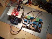
I have the B1 crossover running off the regulators of my DCB1 blue edition. The crossover is drawing around 200mA per rail, so I currently have the CCS of the DCB1 running at 420mA. I achieved this by paralleling a 5R1 resistor to the existing 10R resistor, effectively creating a 3R3 resistance, which is dropping 1.4V. I will probably increase the current once I fit bigger heatsinks, but for testing it should do fine.
I'm afraid there may be more to the offset than just mismatched JFETs, because the offset varies when I move around the output wires. I terminated all outputs with 20k and shorted the input.
Maybe fitting decoupling caps will make the circuit more stable.
I'm afraid there may be more to the offset than just mismatched JFETs, because the offset varies when I move around the output wires. I terminated all outputs with 20k and shorted the input.
Maybe fitting decoupling caps will make the circuit more stable.
Attachments
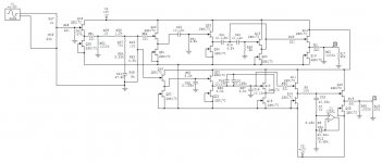
Does anyone see any apparent issues with this implementation?
I notice quite a few superfluous resistors, and Q18. 19, 21 and 46 need
Gate stoppers.

Some of the resistors in the schematic, like R47/46 (volume), R36/37 (bsc), or R49/53 (LF level) are actually potentiometers. The resistors around them are there so I can use lower value pots, limit the pots' range and hopefully increase precision and temperature stability.
I'm also sorry for the awkward part numbers.
I'll add more gate stoppers, I was hoping that with keeping paths as short as possible I could without them.
And maybe I'll admit defeat and add a 10u cap at the LF output...
Oh, and I attached what I hope is a less fuzzy version of the schematic, same awkward part numbers though.
Attachments
 ,
,Thanks Papa Pass! The gate stoppers did the trick! 
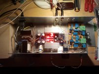
The circuit is up and running, and the output offsets are now all close to 1mV (-0.6mV/1mV for the HP, -1.6mV/0.9mV for the LP, left/right channel). I have it playing with the input volume control at 12 o'clock right now, so there is enough gain in my system it seems, no additional gain stages required
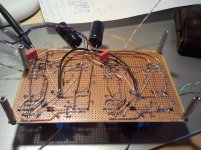
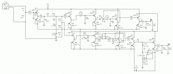
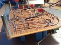
The final circuit is like the one I posted earlier, but with 221R gate stoppers at each and every gate. And one 2200uF 50V Panasonic FC capacitor per rail for decoupling and peace of mind.
To avoid potential ground loops, the XO's ground is only connected to the DCB1 at one point, namely through the cables coming from the power supply. Since the circuit is biased in class A I see no potential harm in doing so.
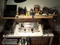
It may not really look like it, but this may be the quietest circuit I have ever built. Even with getting the ear right up to the speaker, one can barely tell if the B1XO is on or off.
And the sound/performance is everything I had hoped for. This circuit would definitely be worthy of a real proper pcb! And a lot less work too...
So, thanks guys for putting this together, and also for helping me with troubleshooting!
The circuit is up and running, and the output offsets are now all close to 1mV (-0.6mV/1mV for the HP, -1.6mV/0.9mV for the LP, left/right channel). I have it playing with the input volume control at 12 o'clock right now, so there is enough gain in my system it seems, no additional gain stages required
The final circuit is like the one I posted earlier, but with 221R gate stoppers at each and every gate. And one 2200uF 50V Panasonic FC capacitor per rail for decoupling and peace of mind.
To avoid potential ground loops, the XO's ground is only connected to the DCB1 at one point, namely through the cables coming from the power supply. Since the circuit is biased in class A I see no potential harm in doing so.
It may not really look like it, but this may be the quietest circuit I have ever built. Even with getting the ear right up to the speaker, one can barely tell if the B1XO is on or off.
And the sound/performance is everything I had hoped for. This circuit would definitely be worthy of a real proper pcb! And a lot less work too...
So, thanks guys for putting this together, and also for helping me with troubleshooting!
Attachments

.........The low pass multiplies all the offsets from each stage, resulting in a net output offset.
So nothing to do with accumulation of offsets.Thanks Papa Pass! The gate stoppers did the trick! ........... and the output offsets are now all close to 1mV (-0.6mV/1mV for the HP, -1.6mV/0.9mV for the LP, left/right channel).................
The final circuit is like the one I posted earlier, but with 221R gate stoppers at each and every gate. And one 2200uF 50V Panasonic FC capacitor per rail for decoupling and peace of mind...........
It was jFETs lacking gate stoppers.
Thanks for the warning.
So nothing to do with accumulation of offsets.
It was jFETs lacking gate stoppers.
Thanks for the warning.
Some additional detail on that:
Like I said, the problem was mainly present in the low pass (LP) section. It didn't matter if I had the circuit powered from a somewhat wonky regulated benchtop PSU or the DCB1's regs, the output offset of the LP was somewhere between +100mv to +150mV. There also was a 5mVpp high frequency fuzz going on, but I didn't pay too much attention to it. the high pass section was doing fairly well. At this point the circuit was exactly like in post #271, with gate stoppers only at points I thought were crucial. The decision to do so was partly motivated by your post #214, AndrewT
What was suspicious though was the fact that the output offset changed with the orientation of wiring and touching the cases of the caps. It also changed with waving the hand over the circuit, definite red flag. In hindsight this makes sense I guess, since, without gate stoppers, the JFETs in the LP pretty much only see a capacitance to ground, and this high impedance will cause problems no matter how short the wiring is.
With gate stoppers for each and every gate the circuit is stable and very, very quiet.
So, the lesson, dear reader: Make liberal use of gate stoppers.
What is being achieved by that? As can be seen in the 2sk170's datasheet, at V_DS=10V the input capacitance C_iss is 30pF. Together with the 221R gate stopper resistor this is effectively forming a high pass with -3dB at f=1/(2pi*R_gate*C_iss)=24MHz. That's unexpectedly high.
...
A filter feeding into B1 should not have anything between the filter output and the very high input impedance of the B1. Do not add any of the Rin setting components and/or band limiting filters that are used in a standard pre-amp/buffer.
I guess I read that as "just use a pair of naked JFETs". Clearly didn't work.
Use your gate stoppers, folks.
- Status
- This old topic is closed. If you want to reopen this topic, contact a moderator using the "Report Post" button.
- Home
- Amplifiers
- Pass Labs
- B1 Active Crossover