Hello,
Especially if the two RG400 cables will leave your chassis to be connected to another '' collection of printed circuits it would be mandatory to use some kind of strain relief before leaving the chassis.
My DDDAC chassis is heading to 40 kilo so without strain relief all force will be on the soldering joint and on top of that the force will be on one side and not pulling in a straight line away from the print.
Many of us will have a spaghetti of dangling wires in open air waiting for something bad to happen.
Greetings, eduard
Hello!
I have RPi4 + FifoPi + ES9038Q2MDualMono + LL1544A TransformerIV with 510 Ohm
It works well with the my current amplifier with RCA input.
The problem:
I finished a test version of a new symmetrical DIY A class amp and it has both RCA and XLR input also.
If using the RCA input, the volume is normal and acceptable but from XLR is very-very quiet.
Any idea?
Maybe necessary the schematic of amp:

and looks like:

Thank you in anticipation
Gyuri
I have RPi4 + FifoPi + ES9038Q2MDualMono + LL1544A TransformerIV with 510 Ohm
It works well with the my current amplifier with RCA input.
The problem:
I finished a test version of a new symmetrical DIY A class amp and it has both RCA and XLR input also.
If using the RCA input, the volume is normal and acceptable but from XLR is very-very quiet.
Any idea?
Maybe necessary the schematic of amp:
and looks like:
Thank you in anticipation
Gyuri
Thanks Ian, for continued investigation on how to get the best clock solution for the FiFoPi. Looking forward to your ideas and observations.
In the meantime, I got my Accusilicon 338 series. I will do testing soon after they are a few days on power….
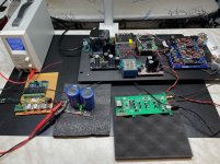
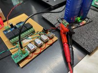
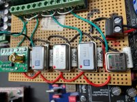
To make sure, when comparing clocks, all clocks are „warm“, I needed to make a small solution. See the pics…. It is like a clock warm keeper and the Bluetooth selector will enable real A_B switching from the listening position (smartphone app controls the 4 relays) - so 4 clocks can be compared all at once without any clock being unpowered ….
I am using your UC-conditioner and linear pi for the testing….
Will report back my view of things
In the meantime, I got my Accusilicon 338 series. I will do testing soon after they are a few days on power….
To make sure, when comparing clocks, all clocks are „warm“, I needed to make a small solution. See the pics…. It is like a clock warm keeper and the Bluetooth selector will enable real A_B switching from the listening position (smartphone app controls the 4 relays) - so 4 clocks can be compared all at once without any clock being unpowered ….
I am using your UC-conditioner and linear pi for the testing….
Will report back my view of things
Attachments
Any idea?
Just a thought:
Is the XLR signal ground referenced at the source end? Is the source a transformer? If so, is secondary winding center tap grounded?
Also, do you have a scope?
Doede @
I have Accusilicon 338, and I almost gave them up, but after awhile they settle in. I really like them now. Looking forward to hear what you think about them.
thanks for heads up, how long did you have them on power continuously?
Just a thought:
Is the XLR signal ground referenced at the source end? Is the source a transformer? If so, is secondary winding center tap grounded?
Also, do you have a scope?
Sorry to interfere, Not my thread, but I know this can blow away the fifopi discussions - this amplifier debugging is worth a thread on its own
just my 2 cents
STS sine to square converter board signal quality measurement
DACs take the clocks in square waves, not in sine waves. So the sine to square wave converter is also very significant. DACs are a kind of digital logic. Clock Jitter for a DAC is decided by the edges of the clocks, not the phase of the sine wave. The DAC performance can be degraded if the quality of the square wave is not good enough, even if it is already with very good close-in phase noise.
I had big hopes for TWTMC-DIRXO with SC-cut crystal because the sine wave phase noise measurement results were very good. However the square wave jitter measurement result was not as good as I expected. So I did more tests to the STS square wave outputs in the time domain. Please find the waveform results attached. Left is STS output waveform, and the right is the CCHD957 output as reference.
Hi Ian,
Thanks for the thorough testing and the detailed description. (already 4 parts, and i guess some more will follow)
Wow, the output waveform of the STS looks really bad. The device on the STS is a U74AC04G, which is a simple
hex inverter, which is steep to accept sine wave and by the looks of it, it doesn't work properly.
Andrea´s TWTMC-STS-FSDO Sine to square converter uses the LTC6957, which is a much more suitable device.
( although at ca. 7,50€, quite costly)
i have few suggestions about your test setup:
i noticed that you testet the bare PCB of the TWTMC, please don't, put it in a case, especially when there's a
computer on the same desk. and i think 2 days of burn in is not enough, the TWTMC (...as any other proper clock)
needs 2 to 3 days to warm up to reach peak performance, alone
IMO the TWTMC with it's large PCB and the many discrete parts is much more sensible to outside influences
than the other integrated clocks like the CCHD957.
And i suggest that you rethink your listening test. Imho it's difficult to hear differences in clocks, when the
I2S signal gets altered that much between the source and the DAC-chip.
the buffer on the HDMIpi will add some jitter as well as the HdMI-cable itself, and also the input buffer in the Topping D90.
and to my knowledge the D90 does some reclocking by itself. it seems that the D90 uses a pair Accusilicon clocks and
a CPLD ( only a CPLD and no flip-flops...)
Thanks Ian, for continued investigation on how to get the best clock solution for the FiFoPi. Looking forward to your ideas and observations.
In the meantime, I got my Accusilicon 338 series. I will do testing soon after they are a few days on power….
To make sure, when comparing clocks, all clocks are „warm“, I needed to make a small solution. See the pics…. It is like a clock warm keeper and the Bluetooth selector will enable real A_B switching from the listening position (smartphone app controls the 4 relays) - so 4 clocks can be compared all at once without any clock being unpowered ….
I am using your UC-conditioner and linear pi for the testing….
Will report back my view of things
Wow, that's a cool setup !
i´m looking to your testing....
thanks for heads up, how long did you have them on power continuously?
I use to turn on my hifi when I am home after work, and turn it off 5-6 hours later. Two- three evenings should be enough I guess.
Thanks for this series: "Trying to get the most out of TWTMC clocks for FifoPi system". It's a classic read.
I'll be in for a squarer.
My goal for desktop is just "DIY training / education", so just hoping to get things functioning this year. After that will be fine tuning, so the squarer and UcPure down the road fits into that timeline.
I'll be in for a squarer.
My goal for desktop is just "DIY training / education", so just hoping to get things functioning this year. After that will be fine tuning, so the squarer and UcPure down the road fits into that timeline.
Hello ,
Ian told us it would be a nice upgrade .
I will give this board its own lifepo4 cell with an UcHybrid board.
You will have to remove L1 on the backside of the reclockpi in order to give the board its own power supply using the J4 connector.
Giving the STS boards from Andrea also their own supply is a bit more '' tricky ''
Greetings, eduard
Thanks for sharing @wlowes
I guess I need to plan for another 3.3V UcHybrid when I'm at the fine tuning stage.
I wonder if supplying dedicated power to the potential squarer will also improve things. Ian usually has this option by default on his products, so guessing the squarer will likely have this option too.
I guess I need to plan for another 3.3V UcHybrid when I'm at the fine tuning stage.
I wonder if supplying dedicated power to the potential squarer will also improve things. Ian usually has this option by default on his products, so guessing the squarer will likely have this option too.
Hi Ian,
every kind of DAC (R2R or delta-sigma) switches on the edges of the clock and not on the upper or lower steady state of the square wave.
So the ringing does not matter unless it creates meta-stability, that's not the case.
Unless they are too slow the rising and falling time of the clock don't affect the digital to analog conversion.
As I already said what really matters is the fluctuation of the time interval between the edges, which creates the jitter.
Unfortunately the beauty of the wave form does not improve jitter.
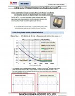
Just to confirm that beauty of the waveform and crazy speed rising and falling edge don't matter I attach the first page of the NDK DuCuLon OCXO datasheet.
The picture at the bottom-left of the page is the HCMOS Output wave of the OCXO, the same output type of the STS.
It has ringing and bounce and looks very similar to the one of the STS.
The picture at the bottom-right of the page is the Bipolar Driver Output wave of the OCXO wich performs a little better in the phase noise plot published by NDK.
The slope of the edges are very inclined therefore rising and falling time are very long.
This OCXO was especially design for audio by one of the most important company of the market and it's priced around USD 1600.
As you can see they didn't care much about the beauty and the edge speed of the waveform although the oscillator was designed specifically for audio applications.
Sorry to repeat again but you are using a tool suitable for measuring the jitter with an integration bandwidth useful for telecommunication applications, with a time base probably worse than the DUT you are measuring.
There is no way to overcome this limitation in software because your digital oscilloscope does not use cross correlation to do the math.
So, as I have said several times, likely you are measuring the noise floor affected from the noise of your tool.
That's the reason why even NDK has published the phase noise plot measured by a suitable tool like a phase noise analyzer, rather than the jitter captured by a digital oscilloscope..
If you would perform accurate measurements I would suggest to buy a phase noise analyzer like the Microsemi 5120A or the Aeroflex PN9000 which there are the cheapest tools for this, although I believe they are priced 25-30000 USD for a new one.
You could look for a used one, or maybe you could build yourself the Holme project to save thousands USD, I believe you can build it with less than 2000 USD.
Andrea
every kind of DAC (R2R or delta-sigma) switches on the edges of the clock and not on the upper or lower steady state of the square wave.
So the ringing does not matter unless it creates meta-stability, that's not the case.
Unless they are too slow the rising and falling time of the clock don't affect the digital to analog conversion.
As I already said what really matters is the fluctuation of the time interval between the edges, which creates the jitter.
Unfortunately the beauty of the wave form does not improve jitter.
Just to confirm that beauty of the waveform and crazy speed rising and falling edge don't matter I attach the first page of the NDK DuCuLon OCXO datasheet.
The picture at the bottom-left of the page is the HCMOS Output wave of the OCXO, the same output type of the STS.
It has ringing and bounce and looks very similar to the one of the STS.
The picture at the bottom-right of the page is the Bipolar Driver Output wave of the OCXO wich performs a little better in the phase noise plot published by NDK.
The slope of the edges are very inclined therefore rising and falling time are very long.
This OCXO was especially design for audio by one of the most important company of the market and it's priced around USD 1600.
As you can see they didn't care much about the beauty and the edge speed of the waveform although the oscillator was designed specifically for audio applications.
Sorry to repeat again but you are using a tool suitable for measuring the jitter with an integration bandwidth useful for telecommunication applications, with a time base probably worse than the DUT you are measuring.
There is no way to overcome this limitation in software because your digital oscilloscope does not use cross correlation to do the math.
So, as I have said several times, likely you are measuring the noise floor affected from the noise of your tool.
That's the reason why even NDK has published the phase noise plot measured by a suitable tool like a phase noise analyzer, rather than the jitter captured by a digital oscilloscope..
If you would perform accurate measurements I would suggest to buy a phase noise analyzer like the Microsemi 5120A or the Aeroflex PN9000 which there are the cheapest tools for this, although I believe they are priced 25-30000 USD for a new one.
You could look for a used one, or maybe you could build yourself the Holme project to save thousands USD, I believe you can build it with less than 2000 USD.
Andrea
Attachments
Last edited:
"Unless they are too slow the rising and falling time of the clock don't affect the digital to analog conversion. As I already said what really matters is the fluctuation of the time interval between the edges, which creates the jitter. Unfortunately the beauty of the wave form does not improve jitter."
+1
Sometimes overdamping at the clock line termination improves sound quality. Mostly done in practice if using source series termination. Sometimes the technique can be seen in commercial dacs.
+1
Sometimes overdamping at the clock line termination improves sound quality. Mostly done in practice if using source series termination. Sometimes the technique can be seen in commercial dacs.
Last edited:
- Home
- Source & Line
- Digital Line Level
- Asynchronous I2S FIFO project, an ultimate weapon to fight the jitter