Hi!
The theory of the filter hasn't been completed yet, because a predictor should be used for stability. It might be done with time delay, but I will think about it at this summer. Up to that time:
John, don't you want to share with us the schematics of the amp.? Then everybody could learn from his own, and each other's mistakes..
Gyula
The theory of the filter hasn't been completed yet, because a predictor should be used for stability.
It might be done with time delay, but I will think about it at this summer. Up to that time: John, don't you want to share with us the schematics of the amp.? Then everybody could learn from his own, and each other's mistakes..
Gyula
Attachments
Synchronous regulator for PowerDAC amp
Hi everyone
I've seen a lot of interest in this thread on volume control of an all-digital amplifier by means of PSU voltage control, as is done in the TacT Millenium. This strategy has the advantage of preserving the dynamic range at all volume settings and reduces losses at low volumes. Another plus is that for much of the time the power output stage components will be operated at a minimum stress level which improves reliability.
I've implemented this method in my PowerDAC 1 and PowerDAC 2 digital amplifiers and I've posted below the circuit of the regulator used in the PowerDAC2 in case it be of interest to members. (Don't panic; it's not nearly as complex as it first looks!)
The synchronous regulator uses average current mode control and has a novel feature: The equations for optimising the control loop for ACM control (as per Unitrode appnote by Lloyd Dixon) are a function of the output voltage. Thus it's difficult to design an ACM controlled regulator with a variable output voltage that's optimal at all output voltages. This problem is overcome in this design by changing the Current Loop Gain as a function of the Reference Voltage, using a video VCA, in such a way that the current loop control is optimal for all output voltage settings from 2 to 60V.
The regulator feeds off a raw +75V supply and is rated at 2-60V at 6A continuous. Output voltage is directly proportional to the Reference Voltage 0-5V. The latching current overload trip is set at 7.5A. Control voltages of +5V, +12V and -12V are required. Provision is made to lock the switching frequency to an external 176.4kHz reference derived from the audio clock system. If this is not used, the switching frequency will default to free running at about 0.9 x 176.4kHz.
In the PowerDAC2 amplifier, each channel has one of these switching regulators and the Reference Voltage is obtained from the DAC port of a supervisor microcontroller; the micro uses a Lookup Table to generate the required voltage for a log volume taper. But probably the simplest arrangement would be a log taper pot, but provision should be made for limiting the slew rate of volume change. (and also for limiting the voltage rise on the raw supply when volume is rapidly decreased.)
The regulator should ideally be supplied with the three control voltages prior to the +75V raw, but circuitry has been provided with secondary UVLO to ensure a safe condition should this not be possible.
These regs have now been in service for 2 years and have proved robust. If anyone is interested, I also have a beefier (for driving two power output stages) synchronous reg circuit which uses voltage mode control and is somewhat simpler.
John Hope
Attachments
Hi John!
Thank you for the supply! Wasn't there a problem from the FETs are in lack of schottkies? I think there is too big Qrr for 176 kHz. How did you proportion the transfer function?
Comments to the earlier post: I think the analog linear phase filter with the input time delays acts as 'predictors' will form a discrete FIR filter.
Gyula
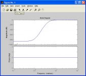
SyncReg Control Loop
Hi Gyula again:
I managed to locate my design notes - such as they are - for the SyncReg. The control loops design is based on a procedure described by Lloyd Dixon in Unitrode Application Note 140 'Average Current Mode Control of Switching Power Supplies. The stuff below should make sense in the context of this article.
Following Dixon's method, the ratio of the otimum Current Loop gains for Vo=2V and Vo=60V is 30. So the current loop was designed for a Gca=1.317 at 60V and the VCA - controlled by Vref -attenuates the feedback so as to increase the gain to Gca=39.51 at Vo=2V. 25% of the total gain budget has been allocated for the outer voltage control loop, so the Gca at 60V has been reduced to 1.0
The current loop amp has a zero placed at f(ci) = fs/(2.pi) = 14kHz and a pole at fs=176400.
The voltage loop gain is fixed at Gva = 11.8. (from slope matching at fs).
The voltage loop amp has a zero at f(ci) = 28kHz.
Hey Gyula, it's been a while since I looked at this stuff and I think I just overheated my brain!
Cheers
John
Hi John,
nice design. I wonder if you could use UC3841 PWM regulator instead of VCA for current loop gain control. UC3841 uses pwm ramp voltage feedforward, so you do not have to change current loop gain to compensate for current waveform downslope steepness change with output voltage. I have no personal experience with UC3841, but I did a design once with it's precedessor UC1840 and it worked as advertised.
Best regards,
Jaka Racman
UC3841
Hi Jaka
Yes it certainly would be worth investigating this because I see that the Elantec VCA has been discontinued. I have a little box full of them, though. How often our design decisions are dictated by what we can get, eh? In any case a reduction in component count would be a good thing.
I've attached the simpler (and older) voltage mode control sync reg I use in PowerDAC1. This syncreg also supplies 2-60V but at a max current of 12A and so can be used for both channels of a stereo amp. Switching frequency is 88.2kHz and there is a non-latching overcurrent trip. The circuit has been in use for five years with no problems, but with the benefit of hindsight I would suggest that anyone wanting to build this circuit would improve and simplify it as follows:
1. The output FETs are gross overkill (I had samples, so...) and should be replaced with something like IRF3315 or (if the raw supply is TransZorb clamped to 90V or less) the new IRF540Z.
2. The gate driver configuration with its need for a floating supply is also overkill and the IR2110 could be used on its own in a bootstrap configuration, as is done in the more recent syncreg. This would necessitate an alternative cycle by cycle current limiting strategy, though.
If the syncreg would be used on a raw voltage less than 60V, one of the 'adaptive' gate drivers from Linear Tech could be used, which would replace the IR2110 and all the drive conditioning.
Having said all that, the output stage with the massive FETs and the adaptive drivers is almost indestructible. I use the PowerDAC1 amp as a test bed for various prototype designs and as such the syncreg is subject to terrible abuse. It's never let me down.
3. If a less 'sledgehammer' output stage is used, and the gate drive does not allow both FETs fully off for any time, then the bypass UFast diodes could probably be omitted with little impact on efficiency.
4. The LEM current sensor is expensive and wasted on this simple 'trip' function. One could use a low valued shunt or something elegant like a GMR sensor (NVE AA series) over a pcb trace)
5. Although it works OK with reasonable delta load response I've never been totally happy with the control loop. . The values I calculated on paper had to be 'tweaked' significantly for stability over the whole output voltage range. Needs revisiting....
I hope that these circuits could form a useful basis for some good DIY sync reg designs for digital amplifiers.
Regards
John H
Hi Jaka
Yes it certainly would be worth investigating this because I see that the Elantec VCA has been discontinued. I have a little box full of them, though. How often our design decisions are dictated by what we can get, eh? In any case a reduction in component count would be a good thing.
I've attached the simpler (and older) voltage mode control sync reg I use in PowerDAC1. This syncreg also supplies 2-60V but at a max current of 12A and so can be used for both channels of a stereo amp. Switching frequency is 88.2kHz and there is a non-latching overcurrent trip. The circuit has been in use for five years with no problems, but with the benefit of hindsight I would suggest that anyone wanting to build this circuit would improve and simplify it as follows:
1. The output FETs are gross overkill (I had samples, so...) and should be replaced with something like IRF3315 or (if the raw supply is TransZorb clamped to 90V or less) the new IRF540Z.
2. The gate driver configuration with its need for a floating supply is also overkill and the IR2110 could be used on its own in a bootstrap configuration, as is done in the more recent syncreg. This would necessitate an alternative cycle by cycle current limiting strategy, though.
If the syncreg would be used on a raw voltage less than 60V, one of the 'adaptive' gate drivers from Linear Tech could be used, which would replace the IR2110 and all the drive conditioning.
Having said all that, the output stage with the massive FETs and the adaptive drivers is almost indestructible. I use the PowerDAC1 amp as a test bed for various prototype designs and as such the syncreg is subject to terrible abuse. It's never let me down.
3. If a less 'sledgehammer' output stage is used, and the gate drive does not allow both FETs fully off for any time, then the bypass UFast diodes could probably be omitted with little impact on efficiency.
4. The LEM current sensor is expensive and wasted on this simple 'trip' function. One could use a low valued shunt or something elegant like a GMR sensor (NVE AA series) over a pcb trace)
5. Although it works OK with reasonable delta load response I've never been totally happy with the control loop.
. The values I calculated on paper had to be 'tweaked' significantly for stability over the whole output voltage range. Needs revisiting....I hope that these circuits could form a useful basis for some good DIY sync reg designs for digital amplifiers.
Regards
John H
Attachments

Variable switching power supply
Hi guys
There is another variable switching power supply (2-40V, 12A) in TI's application note Implementation of Power Supply Volume Control. It uses UC3849.
John,
How did you manage volume control at low levels (since the output voltage of the power supply can't go down to 0V)? Do you use some kind of attenuation in digital domain? I was thinking about using power supply volume control for 0 to -26dB (40-2V) and digital attenuation with SRC4193 asynchronous sample rate converter below -26dB.
Another idea is to use a switcher as tracking preregulator for some kind of linear regulator. This way the voltage difference between the linear regulator's input and output is constant, hence power dissipation is reasonable across the entire output voltage range. Also, it is possible to make the linear regulator to go down to 0V.
Have anyone a schematic of GOOD linear regulator (0-40V, 10A) with very low output impedance (few miliOhms)?
Dejan
Re: Variable switching power supply
Hi Rookie
The PSU shown in the SLEA038 have extreemly low output impedance - a few mR over the complete audio band when used with a amplifier board with 6x1000uF ZL caps from Rubicon.
This supply can also sink current - aprox 3A - and is therefore very good when used together with the TAS5518 modulator (use the PSVC output to control the voltage)
As explained in the SLEA038 the TAS5518 can control the PSU, and can be set to have 12, 18 or 24dB variation of the PSU voltage and then uses the digital gain/attenuation before and after the PSU.
Having lower voltages than 2-3V is not feasible, because then you get a feed from the gate-capacitances to the drain nodes.
rgds,
Kim
Hi Dejan
If you do use a linear post regulator, then make sure that the linear regulator also can sink current!
As I recall the SCR4193 is not able to gain digitally, and you really need that with a lot of CD's and DVD's. The TAS5518 has plenty of digital gain - up to 36dB and also contains a digital audio processor with 7 biquards pr channel - a very easy way to do cross-over for active speaker systems.
Also I think the TAS5518 with the use of AD-modulation is easier to design with - and it should also be a lot cheaper - only problem is that you need a kind of microcontroller to send the I2C.
TAS5015 has a DYR of around 107dB in a normal application, whereas the TAS5518 have 112dB - and that with a build-in PLL and on all 8channels.
Comparing the sound of the TAS5015 to the TAS5518 is not easy as both modulators are very good, I personally prefere the TAS5518 with it's more smooth sound - probaly due to less cross-over distortion from the AD-mode modulation.
TI will soon release a new EVM with the TAS5518 and TAS5182 mosfet driver. 8x 150w @ 4R
rgds,
Kim
SyncRegs
Hi Rookie
In PowerDAC 1 and 2 I follow a similar scheme to that used by Tact in the Millenium; that is PSU voltage control from 2 to 60V and digital attenuation below 2V.
What you propose seems OK.
The idea with a switching preregulator is interesting, but I don't really see the need for it. High frequency ripple is not really an issue in this application; what's important is LOW output impedance and FAST response over the whole audio bandwidth. This can easily be accomplished with a well designed switcher.
For small signal control the loop bandwidth should be of the same order as the audio bandwidth (2x if using a bridge OPS, actually). This can be accomplished by using average current mode control with optimised control loop parameters.
For transient response, it's LARGE signal parameters which matter most, since the control loop will likely be against the stops anyway. This is partly determined by the rate at which the inner (current) loop can slew and is related to inductor value and duty cycle. The capacitance value of the reservoir cap also affects transient response, as it is the first 'port of call' for load current demand is the reservoir cap. Small caps here will not be helpful.
What is helpful when designing for transient response is that the load current of the regulated PSU is slew-limited by the digital amplifier's baseband frequency response, and true 'step changes' of current will not occur. You can work out what the maximum change in load current will be and use that as a design parameter.
TI has several appnotes on loop design in general and average current mode loop designs in particular. Seek out anything written by Lloyd Dixon. Once you understand it (which took me ages but then my information osmosis rate is very low) it's very rewarding to build a PSU and go measure the responses of it and find they're not far out from what you calculated.
Hope this helps
John
Kim,
As I understand TAS5015 operates in both AD an BD mode. If only the AP and AM outputs are used (AP -> upper left side and lower right side of the bridge, AM -> lower left and upper right side of the bridge) the amplifier operates in AD mode. If all of the outputs are used (AP -> upper left side, AM -> lower left side, BP -> upper right side, BM -> lower right side) the amplifier operates in BD mode. So it is up to user to decide wich type of modulation will use.
Am I right, or maybe I'm missing something?
John,
I saw your designs of power supplies and it's apparent that you put much effort in the design. I will go easier way and use the power supply from slea038. But that will wait for a while, because my prime concern now is my final project.
Regards,
Dejan
Dejan
It is correct that you can operate the TAS5015 in AD-mode, but then you do not get the high DYR, because the TAS5015 do not contain compensation for the 2'order unlinarity from the conversion from PCM to PWM. Noise floor also increases to a DYR of around 98dB A-weighted ( 107dB A-weighted in BD-mode)
This distortion will show up at frequencies from around 1-2kHz and rise linear with frequency.
The TAS5508 and TAS5518 contain compansation for both 2'nd and 3'rd unlinarity and do therefore have low THD in the audio band.
The noise shaper in the TAS5015 and TAS5518 are also different. The TAS5518 noise shaper is chosen to give flat noise floor up to 23kHz, where the TAS5015 rises around 15kHz.
Further the TAS5518 is optimized with better start and stop algorithems so you get lower click during PWM start and stop.
rgds,
Kim
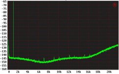
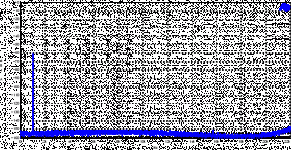
Reclocked / Relatched TAS 5518 DR Atwd greater then 120dB
Note the 0dB scale on both FFT plots is ref. to full power / 0dB output.
As Kim states, note the nice flat noise floor of the 5th order noise shapers in the TAS 5518 - a very good result for an 8Fs AD modulator!
Note the 0dB scale on both FFT plots is ref. to full power / 0dB output.
As Kim states, note the nice flat noise floor of the 5th order noise shapers in the TAS 5518 - a very good result for an 8Fs AD modulator!
Attachments
Dejan
Yes you are right, I work for TI in Copenhagen.
Using the diyaudio site is manily hobby and interesst - not work.
John
you keep impressing me with the measurements you do. Your clock/reclock/relatch circuit makes it possible to see the exact noisefloor of the noiseshaper.
For the TAS5518 with the internal PLL where there is no garantee on the exact timing between MCLK and internal 200MHz clock you must have problems with the reclocker/relatch from device to device.
And yes 120dB from a AD-modulator is good. Adding 24dB PSVC on top => 144dB from clipping to lowest noise.....
With standard integrated output stages and without reclock/relatch a DYR of 110-112dB is normally acheived. Adding the PSVC a pratical DYR of around 130dB is acheived - something most class AB-amps have dificulties acheiving.
rgds,
Kim
- Status
- This old topic is closed. If you want to reopen this topic, contact a moderator using the "Report Post" button.
- Home
- Amplifiers
- Class D
- Anyone interested in a digital amplifier project?