Another amplifier topology from Mr. Jean-Marc Plantefève.
I like the simplicity of that circuit but on simulations the distortion is too high and very dependant on input fets matching.
I like the simplicity of that circuit but on simulations the distortion is too high and very dependant on input fets matching.
An externally hosted image should be here but it was not working when we last tested it.
Hi Jam,
Post 54 has capacitors C-D1 and C-D2, do you know why they are there.
Hi subwo1.
Too many stages - too much phase change within the NFB loop.
Fewer good stages are better, that is where JLH class-A scored, and why I stuck with it.
Hi lumanau,
Couldn't agree more - what you 'see' is not an indicator for what you will 'hear'.
Can I suggest that you run an amplitude plus phase plot to 100MHz with a voltmeter simulated between Q3 and Q7 collectors on subwo1's original circuit.
Off the top of my head I think this will show how the P and N complements do NOT run symmetrically beyond audio frequencies, and that it is the recombination of waveforms at the output devices that cancels distortion.
Is there a point where they become out of phase that would give rise to your oscillation ?
The 2xC+R networks should improve the balance between halves at rf frequencies.
R v CCS. I use R; it has equal linearity at all frequencies.
CCS might offer improvement at low tail currents, and is essential where the differential pair have low value emitter resistors.
Hi Graham,
I agree about propagation delay inside the feedback loop. The emitter followers driving the mosfet gates, though an extra stage, actually lower prop. delay considerably because they speed up gate charge/discharge so much when required by the feedback loop.
Hi thanh,
More heads are better than one.")
I agree about propagation delay inside the feedback loop. The emitter followers driving the mosfet gates, though an extra stage, actually lower prop. delay considerably because they speed up gate charge/discharge so much when required by the feedback loop.
Hi thanh,
More heads are better than one.
Subwo,
thanks for simulating, interesting you didn't note ANY(!?) difference...may it be due to the simulation world limits?
Interesting notes from others saying a resistor instead of CCS sounds better, someone who have made IRL distorsion analysis may tell us about tha harmonics between these two alternatives...?
Maybe it's high time for our heavy weighters on this board...
Lumanauw,
noticed your experience with oscillating poweramp when using a feedback cap, the value of the FB cap should be of such a high value that you may have unit gain at the point when the output is out of phase with let say 60 degrees(Obs! I'm not really sure about this value but I think below 90 degrees anyhow).
Put a Teflon cap trimmer in the FB line and you will get the optimal value.
My own words in general about FB cap if someone want's to use it/need it: I don't think this is an academic question and something that should be calculated to make sense, just do it the empirical way, be happy and listen to your music!
Cheers
Hi, all,
Just want to say this. Although I have notice things about amps, I'm quite behind you guys. I cannot use simulator (wanted to learn). Even I'm not ready to draw schematics using a program. Sorry about this. For discussion, drawings certainly needed to make things clear.
Some days ago, I just experimented with cascoding (the Cascode.pdf from Mr. Pass really gives enlightning, infact every single article he wrote have the highest value, at first I just dont realize it and take it just as an ordinary internet article. Just read every one of them).
I found that cascoding gives much improvement. Dont know if this is contrary to principle of "make amp as simple as possible/use minimal amount of transistor", but in my 3 stages amp, cascoding the differential and cascoding the VAS gives much better audible result.
Want to ask you this. Inspite of cascoding is good, why is cascoding the final stage is "not good" by comments of some expert? In the development stage of A75, Norman Thaggard and Nelson Pass included this final stage cascoding as a choice, but they decided not to use it in the final design due to sound result.
Also I learn this from the forum "Sound of Cascodes" here.
Is it true that cascoding is only can be applied to differential and VAS, at least from the "final sound" point of view? Cascoding every transistor will give better measurement figure, but why cascoding the final stage gives "sterile" sound?
Jam,
Yes, I like that double-diamonbuffer amp too. Although having
more parts it is still a clean and straightforward topology. It might
be suitable for a headphone amp perhaps (or power amp for
those who can afford the heatsinks and electric bills of running
class A ). Maybe one could experiment with a resistor to
ground at the input of the output buffer to reduce the OLG?
As for the Mosquite/Buzquito amp, I was not really thinking of
DC servos (if that is how you interpreted me) but rather something
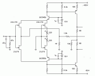
like this, perhaps. The JFETs of the leftmost pair are the input
buffer and have to be closely matched. The rightmost pair looks
like a buffer to, but is two adjustable CCS's which are intended
for bias and DC adjustment since this can no longer be done
at the input buffer. The Rc's of the cascodes will need a lower
value than before since the Iq will be higher, and maybe the
cascode BJTs will need to be replaced with something more
"sturdy". Note, only input and VAS shown in this figure.
Yes, I like that double-diamonbuffer amp too. Although having
more parts it is still a clean and straightforward topology. It might
be suitable for a headphone amp perhaps (or power amp for
those who can afford the heatsinks and electric bills of running
class A
). Maybe one could experiment with a resistor toground at the input of the output buffer to reduce the OLG?
As for the Mosquite/Buzquito amp, I was not really thinking of
DC servos (if that is how you interpreted me) but rather something
like this, perhaps. The JFETs of the leftmost pair are the input
buffer and have to be closely matched. The rightmost pair looks
like a buffer to, but is two adjustable CCS's which are intended
for bias and DC adjustment since this can no longer be done
at the input buffer. The Rc's of the cascodes will need a lower
value than before since the Iq will be higher, and maybe the
cascode BJTs will need to be replaced with something more
"sturdy". Note, only input and VAS shown in this figure.
Attachments
CCS vs. resistor
I am sure some difference in distorsion between CCS's and
resistors will turn up in simulations if sufficiently accurate
models are used. A CCS isn't perfect and even a resistor is
somewhat non-linear. Both devices will also start to behave
differently at higher frequencies.
Leach uses resistor in his amp with the motivation that a
CCS is noisier than a resistor. I don't think CCS's made with
modern components are so noisy that it should matter
except perhaps in low-level applications such as phono amps.
Furthermore, the CCS has the advantage of better PSRR than
the resistor, as has been pointed out, and that probably
dominates over the noise anyway.
These are purely technical considerations, of course, so how
(and if) the two alternatives sound is a different question.
Hi, Graham,
Hi, Subwo1,
I read that you drop the folded cascode. I'm curious about this topology, Q1+Q2+Q7 in your first design. Many design uses this kind of folded cascode configuration, like Mr.Curl, Mr.Borbely, Mr.Pass(in A75), MCIntosh, and so many other.
Usually the differential is more independent to the VAS, only 1 leg of the differential is connected to VAS, but in this design both differential's leg are connected to VAS.
What is the merit of this configuration (compared to old fashioned design)? In measurement? In sound result?
I dont understand this. Got any drawings?The 2xC+R networks should improve the balance between halves at rf frequencies.
Hi, Subwo1,
I read that you drop the folded cascode. I'm curious about this topology, Q1+Q2+Q7 in your first design. Many design uses this kind of folded cascode configuration, like Mr.Curl, Mr.Borbely, Mr.Pass(in A75), MCIntosh, and so many other.
Usually the differential is more independent to the VAS, only 1 leg of the differential is connected to VAS, but in this design both differential's leg are connected to VAS.
What is the merit of this configuration (compared to old fashioned design)? In measurement? In sound result?
Graham,
From my notes about the circuit,
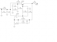
The transresistance RT is high impedance, since this is the input impedance to the output buffer A2 consisting of Q5-Q8. Also this buffer has a voltage gain of nearly unity. The transcapacitance CT is made out of internal capacitances at the input of Q5 and Q6 plus the capacitors CD1 and CD2. These will determine the necessary phase margin to ensure the stability of the amplifier at the given gain and load RL connected to the output.
This thread is getting a lot better than I had hoped. I hope when your amp is ready you might have pc boards available. How about a photo of the prototype?
Argo,
I built the version you posted and there are a few to improve. Try doubling up the j-fets and adjusting the drain resistors. Despite high distortion it does not sound too bad, something you can't tell on a simulator,
Regards,
Jam
From my notes about the circuit,
The transresistance RT is high impedance, since this is the input impedance to the output buffer A2 consisting of Q5-Q8. Also this buffer has a voltage gain of nearly unity. The transcapacitance CT is made out of internal capacitances at the input of Q5 and Q6 plus the capacitors CD1 and CD2. These will determine the necessary phase margin to ensure the stability of the amplifier at the given gain and load RL connected to the output.
This thread is getting a lot better than I had hoped. I hope when your amp is ready you might have pc boards available. How about a photo of the prototype?
Argo,
I built the version you posted and there are a few to improve. Try doubling up the j-fets and adjusting the drain resistors. Despite high distortion it does not sound too bad, something you can't tell on a simulator,
Regards,
Jam
Christer,
You might have something here but I can't see how performance could be much improved.................which brings up our second rule.....to keep it as simple as possible............. (but then again rules are made to be broken).
I think the double diamond buffer would make an excellent output stage in an especially if it is a zero global feedback (I had to clarify this in case Steve Eddy was around ) design.
Here are the rules
1) No Servos
2) Keep the design as simple as it needs to be, without hurting performance.
3) No chip (chump ) amplifiers.............this means you Peter Daniel
4) Keep capacitors to a minimum. (not power supply)
5) Chassis optional and photos encouraged.
I hope when all the designs are completed pc boards will be available so that all members will be able to sample them and most of all this be a learning experience for all of us. Mabe there is a budding designer among us and maybe give the old masters (Pass, Curl and Hansen) a run for their money.... , then again maybe not.
Regards,
Jam
You might have something here but I can't see how performance could be much improved.................which brings up our second rule.....to keep it as simple as possible.............
(but then again rules are made to be broken).I think the double diamond buffer would make an excellent output stage in an especially if it is a zero global feedback (I had to clarify this in case Steve Eddy was around
) design.Here are the rules
1) No Servos
2) Keep the design as simple as it needs to be, without hurting performance.
3) No chip (chump
) amplifiers.............this means you Peter Daniel 4) Keep capacitors to a minimum. (not power supply)
5) Chassis optional and photos encouraged.
I hope when all the designs are completed pc boards will be available so that all members will be able to sample them and most of all this be a learning experience for all of us. Mabe there is a budding designer among us and maybe give the old masters (Pass, Curl and Hansen) a run for their money....
, then again maybe not.Regards,
Jam
Hello lumanauw,
To borrow a phrase, the reports you heard of the demise of the folded cascode for me are greatly exaggerated. The circuit without the cascode was an experimental one for educational purposes only. When I actually build a circuit, the folded cascode one using some value of base input resistors is presently the top contender while the 2nd more conventional one for tests is not even in the running. Thanks for mentioning that those other circuits from well know designers use the folded cascode. Quite honestly, when I discover something, I often do not even know there is already a name for it. I just assumed that since it was such an elegant layout it must have been previously known by someone. I learned that from my _discovery_ of the synchronous rectifier several years ago. I didn't have a name for it so I had a very hard time doing a patent search on it. Also, I played around with the folded cascode about 20 years ago when I was experimenting with the old Tiger amp circuit. In fact, it was in an identical way to how you say it has most commonly been used.
The advantage of applying folded cascode drive from both differential collectors to both VAS emitters is symmetry of operation. A music wave form can have equal chance of a particular excursion in either direction, so it just makes sense to me to enable equal control in both directions. Since cascode drive is faster than base drive, I just figured that it was a way to speed up the feedback loop and give the feedback a forward boost in time. That sounds simplistic, but nonetheless, sums up that aspect of what I was thinking.
To borrow a phrase, the reports you heard of the demise of the folded cascode for me are greatly exaggerated.
The circuit without the cascode was an experimental one for educational purposes only. When I actually build a circuit, the folded cascode one using some value of base input resistors is presently the top contender while the 2nd more conventional one for tests is not even in the running. Thanks for mentioning that those other circuits from well know designers use the folded cascode. Quite honestly, when I discover something, I often do not even know there is already a name for it. I just assumed that since it was such an elegant layout it must have been previously known by someone. I learned that from my _discovery_ of the synchronous rectifier several years ago. I didn't have a name for it so I had a very hard time doing a patent search on it. Also, I played around with the folded cascode about 20 years ago when I was experimenting with the old Tiger amp circuit. In fact, it was in an identical way to how you say it has most commonly been used.The advantage of applying folded cascode drive from both differential collectors to both VAS emitters is symmetry of operation. A music wave form can have equal chance of a particular excursion in either direction, so it just makes sense to me to enable equal control in both directions. Since cascode drive is faster than base drive, I just figured that it was a way to speed up the feedback loop and give the feedback a forward boost in time. That sounds simplistic, but nonetheless, sums up that aspect of what I was thinking.
Jam:
>1) No Servos
>2) Keep the design as simple as it needs to be, without hurting performance.<
I guess both of these leave me out.
>3) No chip amplifiers.<
I admit that unfortunately the vast majority of opamp audio circuits published in magazines and on the web are dreadfully boring. OTOH, opamp circuit can be unique and fun, _if_ the designer is willing to think "out of the box" and devise composite-type circuits. In my own case, I start by assuming that an opamp is not a black box with sealed internals but rather a discrete circuit that is waiting for me to figure out how to get in.
A lot of opamps have compensation pins that provide access to the internal circuit nodes, and you can use these to create interesting composite circuits.
Pins 1 & 8 on many opamps (5534, OP-27 for starters) tap into the bases of the second-stage differential, allowing you to splice in a completely separate discrete input stage (just short the normal input pins 2 & 3 to the minus voltage rails). Gives you great flexibility in setting the input device choice (BJT or FET), input operating currents, degenerative feedback, cascoding, open-loop gain, phase compensation, multiple feedback loops... Different opamps have different styles of compensation nodes, so simply think of what you want to accomplish and look for an opamp that has the internal topology and external access points that you need.
A second example is the AD744/AD811 composite circuit designed by the esteemed Walt Jung, and AFAIR used by diyAudio member Michael Lloyd.
I will include the schematic for a third example (corrected from thread http://www.diyaudio.com/forums/showthread.php?s=&threadid=6328 )
Believe me, there are many other kinds of composite circuits that you can accomplish with opamps.
hth, jonathan carr
Attachments
jam said:
You might have something here but I can't see how performance could be much improved.................which brings up our second rule.....to keep it as simple as possible.............
It is almost as simple.
In the original design, the input buffer serves
two purposes, it is the the input buffer that makes the amp CFB,
but it also (indirectly) sets the bias and DC offset of the OPS.
This latter function motivates the variable source resistors which
add to the buffer Zout. In my suggested mod these two
functions are separated. The intended improvement is a much
lower Zout of the input buffer which makes the whole amp
a more ideal CFB amp and should also make it possible to
lower the values of resistors in the feedback network, which
might further reduce effects of stray L and C. Would it be any
better in practice? I don't know, but it should be rather easy
to fit two extra JFETs and some jumpers onto a PCB so one
can try out both versions. Oh well, somebody will probably
find some flaw in my thinking anyway that I have missed.
BTW, I do really wonder if the original design does work well
in practice regarding output DC, since it doesn't even have a
(Jam, plug your ears
) DC blocking cap in the feedback network(Jam, unplug ears)? To avoid misreadings, my mod would still
suffer from the same problem.
I think the double diamond buffer would make an excellent output stage in an especially if it is a zero global feedback (I had to clarify this in case Steve Eddy was around
With a load resistor as I suggested, then yes I suppose it could
even be a whole ZGF (zero global feedback) amp, at least for
moderate gain like for headphones.
- Status
- This old topic is closed. If you want to reopen this topic, contact a moderator using the "Report Post" button.
- Home
- Amplifiers
- Solid State
- Amplifier Topologies