Hi Graham,
I got back to the original circuit to see what effect your suggestions would have one the simulation. when I removed R3 and R4, none of the other changes seemed to be able to bring the circuit into stability. I thought that connecting the series capacitors between the collectors of the VAS and the bases of the feedback transistors would help, but the only thing which helped was to include R3 and R4.
I seem to find the circuit works best with them given at least 20k values. I even removed the inverted drive of the feedback transistors' collectors to the emitters of the VAS transistors, but that increased the oscillation more.
Hi Lumanow,
Here is more on my thinking about why I thought of using input resistors R3 and R4. They do two things, I think. One is that they delay the input signal so that the feedback can keep up and prevent instability and oscillations. But the original reason I included them is to reduce the current through the input transistors, Q1 and Q6, so that the feedback transistors, Q2 and Q5, can idle with more than half the current. That way, the inverted emitter drive (folded cascode?) on the VAS transistors, Q7 and Q3, is more effective. Its effect is to increase the feedback with less penalty in propagation delay since cascodes have fast response. My thought is that the goal is to make the feedback path as short as possible and as fast as possible. Another benefit of the emitter drive of Q7 and Q3 is to make the idle current of the VAS less sensitive to changes in power supply voltage, reducing the need for the constant current sources on the differential pair emitters. Normally uneven differential transistor currents is considered a source of distortion, but since it permits more feedback on the VAS emitters, it may actually provide a net distortion reduction. Another reason I like this type of VAS emitter drive is that I think it makes the operating point of the VAS transistors more stable by increasing the voltage across their emitter resistors without having to increase their value.
Best Regards
Chris Wood,
Good question. You could use a j-fet cascode but they are not available in higher voltages so bipolars offer more flexibility when higher rails are required.
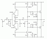
Here is a variant with j-fet cascodes. Mosfets can be used as cascodes as well if you are so inclined. The j-fet version is nifty, because j-fets are depletion mode devices and can be made to self bias and eliminating the biasing circuit. I hope this answers your question.
Good question. You could use a j-fet cascode but they are not available in higher voltages so bipolars offer more flexibility when higher rails are required.
Here is a variant with j-fet cascodes. Mosfets can be used as cascodes as well if you are so inclined. The j-fet version is nifty, because j-fets are depletion mode devices and can be made to self bias and eliminating the biasing circuit. I hope this answers your question.
Attachments
Current sources are highly recommended.") At least the circuit is not quite as sensitive to power supply fluctuations because the folded cascode (?) helps to stabilizze the operating point of the VAS and reduce the tendency of the VAS current to vary. But I do wish to purchase some of those CR470 type diodes. I like to use as few parts as possible since I will probably wire the whole amp p2p.
At least the circuit is not quite as sensitive to power supply fluctuations because the folded cascode (?) helps to stabilizze the operating point of the VAS and reduce the tendency of the VAS current to vary. But I do wish to purchase some of those CR470 type diodes. I like to use as few parts as possible since I will probably wire the whole amp p2p.
Best regards
At least the circuit is not quite as sensitive to power supply fluctuations because the folded cascode (?) helps to stabilizze the operating point of the VAS and reduce the tendency of the VAS current to vary. But I do wish to purchase some of those CR470 type diodes. I like to use as few parts as possible since I will probably wire the whole amp p2p.Best regards
Cascodes And Ccs...
I wondering too how it would affect the differential pair in comparison with a CCS or just a resistor.
Some says that a resistor gives a poor PRSS, ok we fix it with a voltage regulator referenced to GND or whatever! What now....
I suspect the difference between a resistor and a CCS gives a diffrent distorsion with respect to 2:nd and 3:rd overtones etc.
Don't have the equipment to find out but maybe someone perhaps has the answer?
Diff pair with CCS cancels out 2:nd, something to go figure on...
Subwo1,
Please let us know how the design turns out, you might want to build a prototype, circuit boards even.
All,
I am working on changes to the topology I presented (current feedback ) and want to see how far I can improve it.
I hope that everyone that submits a design shares their results. I would like to thank Graham, Subwo1,Thoriated, Lumanauw and everyone that has contributed designs and ideas. The Citation redo looks promising and I hope a schematic gets posted soon. (hint! hint! Millwood)
Regards,
Jam
Hi thoriated,
With a square wave response like that, it looks as if input filtering is not needed !
Hi subwo1,
When you have a differential input stage 91R/2k2 NFB divider resistors will not have signifivant advantage over the more usual 470R/10k. Actually there is a disadvantage because your electrolytic needs to have 5x the 'uF' value.
There is no need to 'bias' electrolytics like that. Tried it - no advantage. Just use a good low esr one.
You have just reported oscillation with my suggestions, and I see that you do not employ any hf output stage damping which is normally applied in the form of a Zobel network. Can I suggest that you try say 22nF and 2.2R in series between output and 0V.
You have further discussed NFB and base resistors. Don't forget that your NFB reference point is at the input end of those resistors, and that transistor capacitance is floating the transistor end when differential base currents only should be flowing. Douglas Self researched input conditions in a recent EW article, and he concluded that amplifier input impedance and resistance should by low.
Hi lumanauw.
JPG attached.
Your real world amp reads good. Power ?
I prefer modern bipolar output devices because there is less device capacitance for the VAS or driver stages to charge during the driving process.
More bipolar current = fatigue ?
Well should be more accurate at higher audio frequencies because there is more current to control internal VAS C-bc.
But equally could reveal more source material flaws, or trigger instability if the design is incompletely compensated.
Changing R16 + 19 ........... yes.
R3 and R4 big ? ????????
Ruins the performance of good input transistors because of additional resistor voltage drop due to transistor Cs. Yes the Cs are small but the input stage must be well controlled for optimum results.
10pF caps + R. I have seen some designers call this feedforward; some nested feedback. It is a method for voltage amplifier stabilisation when followed by a slower current driving output stage, but it is seldom sufficient on its own.
The Q2 to Q3 feedback path ? Oh dear, watch out for transistors letting their smoke out, you can't put it back.
Each amplifier half is actually running independently, but with errors tending to cancel at the output stage. At audio frequencies the halves tend to be in phase, but above 500kHz the device induced phase changes do not coincide and thus cross coupling will cause a high power oscillation.
The capacitor feedback I suggested should be capable of better matching the halves prior to drive combination.
Miller capacitor ?
No this is quite different because one of these components directly induces a 90 degree leading current draw (wrt VAS collector potential) that arises within one half of the otherwise linearly operating differential input stage. Error arises wrt the fixed tail current, instead of being controlled via the differential pair NFB node. This leading 90 current draw effectively turns an amplifier into an low value series inductor. Half a microhenry is common, and this causes propagation delay. The Miller C.dom has a much greater effect upon bipolar output stages than with Mosfets due to the need for sudden VAS bias slew at crossover; it increases bipolar transistor crossover induced artifacts.
Attachments
Jam
Oh, I think the schematic says it all. Some will not like it since
it adds no fancy colouring to the sound, some because it has
no feedback, some because it doesn't even need a PSU we
can argue over. Most will not like it since such a device does
not exist in the real world, but otherwise it seem to be both the
optimal and simplest topology.
(It was posted as a joke, of course, in case somebody missed
that.)
I also like the Mosquito amp, judging purely from the schematic
and my limited knowledge, largely becuause it has a kind
of simple and elegant straightforwardness to it. One thing that
bothers me somewhat, though, is the high value of the source
resistors for the input buffer. I don't quite know what typical
value one will end up setting the pots to, but since they are
200 Ohm ones, I suppose they should be expected to not to
be set very low at least. This would cause the output impedance
of the input buffer to be somewhat on the high side to achieve
"true CFB", but maybe that is even a delibarate design decision
that is supposed to have some advantage? I haven't come up
with any obvious way to fix it though, without modifying the
whole buffer topology. Maybe one could run the JFETs close
to IDSS and use very low Rs values and, if necessary, adjust
the cascode collector loads to compensate for this, but I haven't
tried to dive deep into this issue. Maybe getting rid of the source
resistors alltogether and provide some other means for adjusting
the OPS bias might be a better solution, but once again, it would
increase the complexity. One can also swap the whole
input buffer for a BJT diamond buffer, but some of the elegance
is undoubtely lost then. As a minor thing, I guess it wouldn't
hurt to upgrade the VAS transistors to something more modern
and better.
jam said:
Christer,
Tell us more.................
Oh, I think the schematic says it all. Some will not like it since
it adds no fancy colouring to the sound, some because it has
no feedback, some because it doesn't even need a PSU we
can argue over. Most will not like it since such a device does
not exist in the real world, but otherwise it seem to be both the
optimal and simplest topology.
(It was posted as a joke, of course, in case somebody missed
that.)
jam said:
All,
I am working on changes to the topology I presented (current feedback ) and want to see how far I can improve it.
I also like the Mosquito amp, judging purely from the schematic
and my limited knowledge, largely becuause it has a kind
of simple and elegant straightforwardness to it. One thing that
bothers me somewhat, though, is the high value of the source
resistors for the input buffer. I don't quite know what typical
value one will end up setting the pots to, but since they are
200 Ohm ones, I suppose they should be expected to not to
be set very low at least. This would cause the output impedance
of the input buffer to be somewhat on the high side to achieve
"true CFB", but maybe that is even a delibarate design decision
that is supposed to have some advantage? I haven't come up
with any obvious way to fix it though, without modifying the
whole buffer topology. Maybe one could run the JFETs close
to IDSS and use very low Rs values and, if necessary, adjust
the cascode collector loads to compensate for this, but I haven't
tried to dive deep into this issue. Maybe getting rid of the source
resistors alltogether and provide some other means for adjusting
the OPS bias might be a better solution, but once again, it would
increase the complexity. One can also swap the whole
input buffer for a BJT diamond buffer, but some of the elegance
is undoubtely lost then. As a minor thing, I guess it wouldn't
hurt to upgrade the VAS transistors to something more modern
and better.
Christer,
J-fets lend themselves to simplicity..............like you said elegant, but I am also working on a version using mosfets............bipolars have too much drift due to base currents.......................and the rules say no servos!
......but to make you happy, you may try this.........
J-fets lend themselves to simplicity..............like you said elegant, but I am also working on a version using mosfets............bipolars have too much drift due to base currents.......................and the rules say no servos!
......but to make you happy, you may try this.........
Attachments
Hi Ultima Thule,
I ran the simulations comparing the resistor with the CCS for distortion. I did not see any difference when the power supplies are rock solid. I am not experienced with all the fancy ways to introduce noise into the circuits. However, I am now convinced that the CCS is worth the trouble since it isolates the emitters of the differential input stage from the noise on the power supply rails as Ultima Thule and thanh know.
Hi jam,
I fear that I may not have a chance to build the amp for quite a while since I am so backed up on other essential projects. But once I can do so, I look forward to providing more information on the project.
Hi Graham, Your ideas panned out. After finagling with the circuit, I have removed the input resistors and then also had to remove the folded cascodes. The differential pairs get fed by constant current and their feedback network is now simplified and easier to operate on higher voltage, which is what I needed to begin with in that case. Basically, the only difference from standard topology after the changes is the Vgs multiplier for bias and the emitter followers for the VAS. The standard phase compensation cap is in the low single digit pF range with a feedback resistor of 10K ohm. The feed forward type capacitive divider does further enhance stability, but it is still very solid. I can't say I find this version special enough though, but it is good to know the various tricks that I have tried out. The distortin figures for 10khz lowered from .04 to .002 while for 100khz they went from .343 to .07. Back to the drawing board or I may try one something akin to jam's ideas.
Regards
My amp runs at +/-36V, and from my personal judgement, it is more nice than full complementary design. Maybe this cannot be simulated, you will have to built one to know. Sometimes what is MEASURED good (or people say it measures good, like low THD, high slew rate, etc) doesn't make good sounding amp. First I dont believe this, always looking for "Hyper Spec" amplifier design, but after building many amp, it is clear to me that "What you hear is not what you measure" (GRollins). And this design is my preference, compared to full complementary.
Subwo1, since you have removed the big input resistor now, is it possible that in your old design, the big input resistor+transistor's internal capacitance produces a LPF so by putting this big resistor your cct doesnt oscilate?
About R VS CCS for feeding differential. Many argued about this, up to now no one can tell which is better. For myself, R loading (but bootstaped with C between 2 half R) gives more pleasant sound, compared to CCS. CCS certainly more acurate, but after the amp is finished, the R loading seems to have more nice sound. But still I cannot put this R loading in my own design. Some designs just HAVE to use CCS. Incase of Subwo1's amp, it can use R loading. But my design have to use CCS, otherwise the DC offset will run crazy.
Graham, your explenation is good, but since I'm an amateur I dont get it all. Why is that this feed forward cap between Q2 base is always have to be connected to Q7 collector? In my experience indeed if we change it to Q3 collector it PRODUCES oscilation. My experiment fits your explenation. But looking at the schematic, both halves, up and down half, are really identical, why should it always attached to upper colector?
One more question. The Feedback resistor sometimes have pf cap parrarel with it. What is the purpose of this? In my other experiment amp, putting this just makes oscilation, instead of eliminating it.
jam said:have too much drift due to base currents.......................and the rules say no servos!
Even when all transistors are on one die?
Oh my, one word can be so important sometimes:
It should say,"it is still not very solid"(in stability).The feed forward type capacitive divider does further enhance stability, but it is still very solid.
- Status
- This old topic is closed. If you want to reopen this topic, contact a moderator using the "Report Post" button.
- Home
- Amplifiers
- Solid State
- Amplifier Topologies