lineup said:
I have no idea.
I only know that Nelson Pass told us to use a HEXFET
for compensation of IRFP240/IRFP9240 MOSFET ( HEXFET, Not Lateral MOS ).
For example IRF610, which is same type.
We should try to find transistor with same thermal characteristics as the output transistors.
NO YOU SHOULD NOT!
Lineup, I do value your contribution in digging up older info on the forum when relevant, but in this case you are doing it by reflex instead of thinking it through - to quote you: 'I have no idea'.
Nelson Pass has given you a solution applicable to a particular topology, and this is NOT it.
This is a CFP output design. Because the output transistors are in a local FB loop, their treshold thermal gradient is compensated by the loop itself, assuming there is current feedback (there are other ways to do it, all MUCH more compensated).
The transistors you need to compensate for are the BJT 'drivers' Q34 and Q35 in the output stage, and these ARE compensated assuming Q25 is closely thermally coupled to them.
Even if this wasn't the casem the output stage uses lateral MOSFETs which have a negative tempco over about 100mA so no compensation would be needed anyway, they do it themselves.
Remember, a CFP 'emulates' the same device as it's input device, in this case BJT (Q34 and Q35), in principle it makes no difference what kind the second (power) device is.
Also, as such, the CFP, being an 'emulation' of a bipolar transistor, typically needs an emitter resistor for thermal stability. In order to apply this correctly to Fab's circuit, we need to identify what the 'emulated emitter' is, and how to apply the rules for a simple (gain of 1) CFP to one with gain.
So, first things first: let's first look at a gain=1 version of the circuit - in fab's case, this would happen if R82, 101, 106, 107 were all removed. A classical CFP would have the emitter of the input BJT connected to the collector/drain of the output device, and this point is the 'emulated emitter'. A 'standard' emitter resistor would then be inserted from that to the output. It is important to understand that it is the emitter of the input BJT that is the local feedback point.
A common mistake is inserting an emitter resistor only in the emitter of the input BJT. This only degenerates the input BJT, not the whole 'emulated' BJT, because now the current through the output device is largely outside the local loop of the CFP - it's influence is only seen by the input BJT by the change in it's collector current. If the output device was a BJT, then there would be some (but instead of the whole CFP output current being fed back to the emitter, only 1/beta of the output transistor current would be seen by the CFP local loop!), but as this is a BJT-MOS CFP, if the output device (MOS) current changes, for instance, due to change of temperature, there is no feedback whatsoever to the input BJT - only indirectly by the extra current acting on the load. This may be enough in a single ended application, but not for complementaries.
Consider this example: in a complementary CFP output with emitter resistors inserted only into the input BJT emitters, what happens if the output device currents increase exactly by the same amount? Given that the output current is the difference between the current through the top and bottom CFP, and the input emitter junction (via series emitter resistors) is at the outou potential, any current passing directly from top to bottom supply rail is COMPLETELY UNSEEN by either CFP local or global NFB!!! This is why inserting emitter resistors ONLY into the input BJT emitters is wrong. Even with the use of lateral MOSFETs, that do not go into thermal runaway (one case where this 'unseen' bias current flows), it is wrong, because any cross-conduction is not seen at all by the amp. In fab's particular case, this is even worse as his CFPs have gain, so this phenomenon can, simplifying things, be said to be able to act (gain times) more.
The proper way to do this would be to connect the drains and emitters as usual, then put a (suitably smaller) 'emulated emitter' resistor for degeneration - this resistor alowes the current of the output device to be a feedback variable, which is essentially what a CFP should be doing.
Now, how do we adapt this to a CFP with gain?
First, we need to retain the ability of the output device current to act as a feedback variable. In order to do this in fab's case, drain resistors have to be included. It is sufficient to tie the drains of the paralleled MOSFETs together and use a single drain resistor per CFP side, as essentially, for the CFP, these are one single node anyway.
Secondly, in order to establish gain, we need to put a suitable divider between the drain, the emitter of the corresponding input BJT, and ground. Important: because the total gain of both devices in the classic (gain=1) CFP is enclosed within the local loop, the equivalent 'emulated BJT' has a very high gm, and consequently very low output impedance. When adding gain to a CFP, remember that you are using current as feedback, so not only is your gm reduced (CFP gain) times and output impedance increased by the same factor to begin with, you have a resistor in series with the output impedance, which is only capable of introducing 1/gain current feedback.
What does this mean? Simply, the CFP will be able to compensate for output device thermal gradient (gain) times less, and the output impedance will be much higher than that of a 'classic' CFP.
For fab's particular case, the first is solved by default by using lateral MOSFETs. The second is, however, exacerbated, because laterals have lower gm, so output impedance is higher to begin with, and so is the CFP's 'open loop gain'. Because of this, less gain is available to be enclosed into the local FB loop, so it would seem prudent to use the least gain on the CFP output stage as possible.
Along with all these basic considerations, there is the need to provide gain in order to be able to compensate for the substantial Vgs needed to fully open up lateral MOSFETs. This voltage is up to 14V, and is limited by the internal gate protection diodes of the laterals. It follows that up to 14V are needed across R44 and R45. From this and the selected gain, we can derive what kind of voltage swing is needed on the emitter resistors of the CFP input BJTs. This voltage swing is essentially what the input stage must provide. It follows that at least half of the total voltage swing must then be present on (R70+R99) and (R100 + R73). BTW, fab, if you are reading this, you forgot to include the bootstrap caps from emitters of Q23 and Q24 to the midpoints of said resistors.
Finally a few notes on the latest schematic:
When this amp clips or gets an output short, the input BJT of the CFP is capable of getting (supply rail)/200 of base current, which means C and E of said BJT will essentially be a 'short circuit', tying the protection zeners from rail to ground via 10 ohm resistor. Something will let smoke out in this case. For starters, locate your protection zeners AFTER the gate stopper resistors of the MOSFET. Secondly, you may not need so low resistances in the first CFP stage and consequently high currents. Thirdly, you really don't need extra buffering as the stage driving the CFP is a follower, so plenty of current available - just use relatively beefy BJTs in the CFP - something with good current gain and perhaps 50-100mA of bias current. Fourthly - i seem to recall mention of driving 2 ohms with this amp? If so, keep in mind that to pairs of MOSFETs will not be able to survive this at 60V rails. They are only 7A devices! Fifthly, the 0.18 ohm source resistors are not going to be very efficient in improving current sharing for laterals, due to their low gm. A value in the ohms range would do that fine, but of course is completely inefficient and impractical. I would suggest some device selection and derating. Because these are laterals, you may do something like finding a best set of three and using them in parallel a situation where you would normally use two if you assumed the two were a perfect pair. Finally, consider input device cascoding, as one of them would be seeing quite a bit of voltage swing on the collector. In order to keep their dissipation roughly equal, and reduce thermal drift, connect the 'unused' side collector to the base supply of the cascoding transistor.
ChocoHolic said:Hi Fab !
... go on and let us know how it is working in real life and if you like the sound.
Your inverting power stage is quite similiar to one of my Rookie designs. Have a look to Rookie G...
The only weak point of this output stage seems to be the fact that the openloop output impedance is high.
But with your additional gain from your complimentary differential input stage you might be able to overcome this, if you find a way to handle the oscialltion issues in real life.
Take especially care for capacitive loads in the range between 50pF and 5nF, because that's a common range of real speaker wires.
Hi Chocoholic
I have done a quick overview of your thread but I am not sure if you have built the Rookie G circuit or only the Rookie H...
Correct me if I am wrong but the open loop gain of the CFP in Rookie G is not that high compared to he close loop gain since the gm of the 2SJ201 is about 4 (typical) if the load can be sometimes about 3 ohms at specific frequencies...The overall gain is therefore somewhat modulated by the load variation. Is it good or bad I do not know but my target is to reduce this variation.
Your Rookie G has a lot of closed gain in the CFP and no drain resistor like suggested by ilimzn for stability purpose.
Thanks for the tips but I always test my amps from 1nf to 2.2uF with 8 ohms in parallel with 10KHz squarewave.
I am not there yet for the sound test but thanks for the interest anyway. I need a lot to do before that but first need to be convinced that it will work. So far everybody seems to be worried about oscillation in such a design with CFP with mosfet. It is true that even microcap simulator detects oscillation depending on slight schanges in the design. Based on the simulator the closed loop output impedance is vey low (at least with my more complex input stage using CFP and caccode).
In fact, I would like to determine the basic rules (amount of gain for each stage, pole compensation, ...) with the members on this forum to design a stable CFP with mosfet (lateral) since it is my second attempt to build one (first one being more than 20 years ago in a lab at school with a passionate professor for audio...).
ilimzn said:
Lineup, I do value your contribution
ilimnz,
thanks very much!
And if you do value my contributions

( do you, honestly speaking ??? )
.... then you better STOP
reading me wrong
and twisting my messages
by ripping sentences out of my REAL MESSAGE
given to my fellow members.
Because if you want to
you can stop miscredit me, and tell the truth instead.
I once had higher thoughts of you
")
Let me get back to do this again, please.
ilimzn
---------------------------------
After some reasoning, in the same post you are quoting
this is advice I gave fab.
And as fab can get the message out of one post
I am sure he got my message.
#########################################
Quote, original written be lineup ... Originally In BOLD, In Strong!
...................................................................................................
The most used bipolar for Q25 in amplifiers,
is the BD139, in TO126 case.
No doubt about this!
So I would try BD139 first.
Let's here what those with practical experience will say.
lineup
....................................................................................................
End Quote by lineup
#########################################
Regards to fab - who knows the facts I tell
No regards dear ilimzn - this time
lineup
Lineup Audio Thermal Investigations
http://lineup.awardspace.com/
fab said:
...The overall gain is therefore somewhat modulated by the load variation. Is it good or bad I do not know but my target is to reduce this variation. ...
sorry to quote myself...but I forgot to indicate that the SKA open loop gain should be also modulated by the load change based on amplifierguru disclosure of his circuit principle where he did not show any local feedback on output...However, many peoples seem to be pleased by the sound of SKA but we know it is a subjective subject....
fab
The elektor hexfet amplifier elektuur
uses same type of output stage!!
... with some gain in output
But uses different MOSFET: IR540 / IRF9540
You may perhaps read that original Elektuur article and
see a bit how that hexfet amp did the thermal tracking
practically
theoretically
ilimzn may may providing us with more than we ever need
Search forum, try find some topics:
- elektor
- hexfet
- IRF540
Regards
lineup
ilimzn said:
[... BTW, fab, if you are reading this, you forgot to include the bootstrap caps from emitters of Q23 and Q24 to the midpoints of said resistors.
Finally a few notes on the latest schematic:
When this amp clips or gets an output short, the input BJT of the CFP is capable of getting (supply rail)/200 of base current, which means C and E of said BJT will essentially be a 'short circuit', tying the protection zeners from rail to ground via 10 ohm resistor. Something will let smoke out in this case. For starters, locate your protection zeners AFTER the gate stopper resistors of the MOSFET. Secondly, you may not need so low resistances in the first CFP stage and consequently high currents. Thirdly, you really don't need extra buffering as the stage driving the CFP is a follower, so plenty of current available - just use relatively beefy BJTs in the CFP - something with good current gain and perhaps 50-100mA of bias current. Fourthly - i seem to recall mention of driving 2 ohms with this amp? If so, keep in mind that to pairs of MOSFETs will not be able to survive this at 60V rails. They are only 7A devices! Fifthly, the 0.18 ohm source resistors are not going to be very efficient in improving current sharing for laterals, due to their low gm. A value in the ohms range would do that fine, but of course is completely inefficient and impractical. I would suggest some device selection and derating. Because these are laterals, you may do something like finding a best set of three and using them in parallel a situation where you would normally use two if you assumed the two were a perfect pair. Finally, consider input device cascoding, as one of them would be seeing quite a bit of voltage swing on the collector. In order to keep their dissipation roughly equal, and reduce thermal drift, connect the 'unused' side collector to the base supply of the cascoding transistor.
Thanks for this quite long description.
The bootstrap caps were omitted for simplification purpose. Anyway, if possible I would like to explore the possibility to avoid them if valuable benefits can be obtained (low feedback design...)
1) Thanks for the fail safe advise regading the zener position. I will have that in mind but not include it yet on my revised schematics.
2) can you explain why not needing high drive current for mosfet in inverting mode compared to follower mode?
3) you mean 50-100 ma of mosfet bias current or drive current?
4) 60V is the power supply voltage of the Hafler DH-200 amp. At 2 ohms the amp power supply will sag for several volts because of excessive current demands. I use regulated 53V front end power supply and the voltage swing due to losses inherent to the design will reduce the possible max output voltage. Have in mind that the zener diodes prevent excessive mosfet gate voltage thus limit the output current (at least for transient periods, this is an audio "music" amp and not steady state amp). Anyway, this is how the DH-200 is designed commercially and it is considered a robust amp. It may be not efficient but works correctly.
lineup said:fab
The elektor hexfet amplifier elektuur
uses same type of output stage!!
... with some gain in output
But uses different MOSFET: IR540 / IRF9540
...
Search forum, try find some topics:
- elektor
- hexfet
- IRF540
lineup
Thanks but the IRF540 is vertical mosfet which is quite different thermally than the lateral one I use...
I have searched the forum but did not find the "schematics" but only discussions.
fab said:
ertical mosfet which is quite different thermally than the lateral one I use...
.. but uses the same output stage
and vertical or not, it is still mosfet
and it is still the same type sziklai output stage using bipolar + mosfet
and a gain of like 2-3, if I remember correctly
------------------------------------------------------------------
I have seen several trustworthy guys at this forum
saying that the thermal behavior of lateral and vertikal
is not that different, like we tend to imagine
not in the end
when it comes down to the practical considerations
and actual build
... now there are different vertcials and different laterals
... so in each case we need to look at this situation
... this is true, fab
------------------------------------------------------------------
i am sure someone will read this
and tell us about ELEKTOR HEXFET IRF540 Amplifier:
1. what transistor was used for thermal tracking
2. what transistors were put onto the Big Main heatsink
My guess ... only the Q25 and the 2 MOSFET, IRF540/9540 were put on main heatsink
And the output drivers Q34/Q35 were on separate smaller heatsinks
lineup
lineup said:
ilimnz,
thanks very much!
And if you do value my contributions
( do you, honestly speaking ??? )
.... then you better STOP
reading me wrong
and twisting my messages
Lineup, you are very good at digging up information from past posts, but some of your posts are confusing. In the same post you give several conflicting things:
1) You do not know (well, I'm sorry - you said it!)
2) Nelson Pass says compensate MOSFETs with MOSFETs (which is confusing because it is correct for most topologies, and there are MOSFETs in this design, but not the type mentioned by Nelson, or in the topology he was talking about)
3) We should compensate the output transistors (in this case it is confusing because the actual output transistors are MOSFETs which makes your statement wrong and potentially dangerous, but the 'virtual' output transistors are BJT's by virtue of using a BJT front end CFP, and you are proposing a BJT for compensation, so it is also right)
4) We should use the same type as Q34 and Q35 (which is indeed correct but confusing because of everything else you said involving MOSFETs, and because you can compensate MOSFETS with BJTs, but not necesairly the other way around)
5) Put Q25 and MOSFETs or Q25, 35, 34 and MOSFETs on a common heatsink (which is actually wrong in both cases, the first suggesting that you indeed failed to notice we are dealing with CFP so Q25 needs to sense temp of Q35 and 35, and definitely NOT MOSFETs because they have the oposite tempco).
So, what is one supposed to think, and how useful will this post ultimately be?
Yes I do value your contribution - so do many other members. You have a wide audience, and this is precisely the reason why you should be very careful what you post, as we all do. Of course, we all make mistakes. But I often feel that in your haste to help people (and I do truly admire and value this because it is very rare), you sometimes get ahead of yourself, and the post ends up making you look like you are trying to be, as we say here, a lid for every pot.
Therefore, even though my previous post is very long (and it does take time and effort to write!), please re-read it, and what I said above. Then re-read what I have quoted from your post, and what you found that I was misquoting. Based on what I read originally, and what you wrote subsequently, I believe I was right in quoting how I did, and warning about possible dire consequences. Let me clear this up:
My problem is not about what transistor you have advised to use, but with this (and this time I will emphasise the exact words):
Originally posted by lineup We should try to find transistor with same thermal characteristics as the output transistors.
And I say, because your post seems to be pointing at the output MOSFETs, NO YOU SHOULD NOT. I think I gave ample reason why not - but I will say it again - this is a CFP, it assumes the characteristics of the INPUT transistor, therefore you do NOT compensate the OUTPUT transistors!!! If you do, especially in the case of using laterals, you end up with thermal runaway. For the same reasons, you put Q25, 34 and 35 on a common heatisnk - the laterals will take care of themselves either way. Getting this wrong is worsened by the original topology fab was using, but he corrected that.
Based on what you wrote, I used what I thought was the most likely interpretation i.e. that you meant the actual output transostors, not the 'virtual' ones formed by the CFP. Your last post seems to confirm this. If so, the principle YOU, not me, spelled out, was incorrect for this topology of the output stage.
If you think I did mis-read your post(s), I appologise and will try to find a english course that improves on 15 years of formal english courses and 33 years of speaking and writing it.
If you think my post is wrong in content, I would appreciate it if you correct me or at least point out my errors.
If you think, like I do, that your original post could be confusing, and lead to incorrect interpretation of what should be thermally compensated, then it is a very simple matter for you to correct yourself, and just be more careful the next time. No problem, we all need to do this every once in a while.
Remember, no-one corrects people that appear to have no idea what they write about - one just ignores them. People correct other people whose opinion they value, otherwise, why bother at all? And, I don't ignore you, and I do correct you... so think about it.
Also, remember that although fab may indeed understand the issue, he is not the only one that is going to read this thread.
Oh, and BTW, its ilimzn, not ilimnz
Source resistors and temperature compensation
I would like to comment on the source resistors. In my amplifiers which also use the common source configuration. I use 12 lateral MOSFET’s in the output stage with no source resistors. I had found that source resistors degrade the quality of reproduced sound in my designs. You may get different results with your design. My designs are usually quite complex and have excellent thermal tracking. My suggestion is to try to eliminate the source resistors and add good temperature tracking circuits to the output stage and drivers. The drivers do not need to be same heat sink as the output devices since there is a mixture of bipolar and MOSFET’s involved. Each requires different temperature compensation to maintain constant idle current over the range of 125 to say 180 degrees within a percent or so. A temperature of about 145 degrees is a nice output stage heat sink temperature to shoot for at idle when running fairly high idle currents for class A operation.
I would like to comment on the source resistors. In my amplifiers which also use the common source configuration. I use 12 lateral MOSFET’s in the output stage with no source resistors. I had found that source resistors degrade the quality of reproduced sound in my designs. You may get different results with your design. My designs are usually quite complex and have excellent thermal tracking. My suggestion is to try to eliminate the source resistors and add good temperature tracking circuits to the output stage and drivers. The drivers do not need to be same heat sink as the output devices since there is a mixture of bipolar and MOSFET’s involved. Each requires different temperature compensation to maintain constant idle current over the range of 125 to say 180 degrees within a percent or so. A temperature of about 145 degrees is a nice output stage heat sink temperature to shoot for at idle when running fairly high idle currents for class A operation.
Re: Source resistors and temperature compensation
Hi
Thanks I will remove the source resistors since I have original matched mosfet from Hafler (DH-200 amp). You seem to succeed in common source but have you used CFP at output?
alaskanaudio said:I would like to comment on the source resistors. In my amplifiers which also use the common source configuration. I use 12 lateral MOSFET’s in the output stage with no source resistors. I had found that source resistors degrade the quality of reproduced sound in my designs. You may get different results with your design. My designs are usually quite complex and have excellent thermal tracking. My suggestion is to try to eliminate the source resistors and add good temperature tracking circuits to the output stage and drivers. The drivers do not need to be same heat sink as the output devices since there is a mixture of bipolar and MOSFET’s involved. Each requires different temperature compensation to maintain constant idle current over the range of 125 to say 180 degrees within a percent or so. A temperature of about 145 degrees is a nice output stage heat sink temperature to shoot for at idle when running fairly high idle currents for class A operation.
Hi
Thanks I will remove the source resistors since I have original matched mosfet from Hafler (DH-200 amp). You seem to succeed in common source but have you used CFP at output?
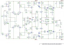
New revised version 0E9
Here it is
I have followed most ilimzn advises but I am still waiting some responses to my last questions.
The amp was too slow, I needed to change compensation cap in differential stage.
I realised that without the bootstrap caps it the feedback may be too low...so I pout 220u at this time (but could be reduced if power-up thump...). Since the feedback was too high and I wanted a flat open loop frequency (audio) response I had to reduce the "natural" input stage gain. So now the feedbcak factor is about 40db. The local feedack output stage gain is now 2.
For now I will put aside the intermediate buffer in the CFP...
I understand that the VBE multiplier should be on same heatsink as the CFP bjt drivers but normally I use separate heatsink for N and P bjt drivers...what could I do?
Please comment.
Attachments
http://www.diyaudio.com/forums/showthread.php?postid=1099995#post1099995lineup said:
2SK134 / 2SJ49 have same data as 2SK1057 / 2SJ161
seems like they are same transistors, basically
...........
missing are the 2SK1530 / 2SJ201 pair
which I think is more powerful at the expense of a bit more capacitance
Toshiba datasheets for 2SK1530 and 2SJ201 at this page
lineup
Originally posted by alaskanaudio, 13th September 2004
2SK1530 and 2SJ201 and excellent combination.
I have been using the 2SK1530 and 2SJ201 combination in all my amplifiers for years.
They are very fine performers when driven properly.
I typically use 6ea 2SK1530 and 6ea 2SJ201 in each channel
in a common source configuration.
Johannes http://www.audioamps.com/
fab,
may be well worth to try the 2SK1530 / 2SJ201
which I mentioned in the above post ( with SK SJ devices overview attachment )
... even if you use two parallel pair of them, like in your circuit
As you can read,
Johannes from Alaskan Audio has got several years of experience of these mosfets.
Regards
lineup
lineup said:
http://www.diyaudio.com/forums/showthread.php?postid=1099995#post1099995
fab,
may be well worth to try the 2SK1530 / 2SJ201
which I mentioned in the above post ( with SK SJ devices overview attachment )
... even if you use two parallel pair of them, like in your circuit
As you can read,
Johannes from Alaskan Audio has got several years of experience of these mosfets.
Regards
lineup
The above lateral SK1530/SJ201 are quite expensive and probably not easy to find them matched. Also, I think their temperature curves are different (high bias point where the temperature coefficient change to avoid thermal runaway...) than the SK134/SJ49 I use.
I know that the SK1530/SJ201 have a higher transconductance than the SK134/SJ49 but for now I rather stay with the mosfet I have until I make it to work and then consider using the above if real benefits can be identified. Thanks for the suggestion
fab said:
Hi Chocoholic
I have done a quick overview of your thread but I am not sure if you have built the Rookie G circuit or only the Rookie H...
Correct me if I am wrong but the open loop gain of the CFP in Rookie G is not that high compared to he close loop gain since the gm of the 2SJ201 is about 4 (typical) if the load can be sometimes about 3 ohms at specific frequencies...The overall gain is therefore somewhat modulated by the load variation. Is it good or bad I do not know but my target is to reduce this variation.
Your Rookie G has a lot of closed gain in the CFP and no drain resistor like suggested by ilimzn for stability purpose.
I have build both and I am listening to both. One on the left chanel, the other on the right
Soundwise prefer the bipolar version. But this comparison is not fair, because the bipolar Rookie H is a three stage amp, while Rookie G is a two stage amp.
Gain:
...well if you only have 4 transistor for the entire amplifier, then you have to live with low feedback.
In case of Rookie G I set the closed loop gain to 25 and feedback factor was about 22db.
Yes gain is varying with the load impedance... good or bad... from point of designing precision equipment bad, from point of designing audiophile equipment... I don't know.
It seems like complex designs do often not sound better, even if they measure better. From my perception there is an optimum in medium complex designs.
This optimum seems not only to touch the sound but also difficulties in R&D.
Below this complexity optimum it is hard to achieve high end performance.
Above this complexity optimum it is becoming more difficult to get it running really proper and handling eventually oscilation issues.
Rookie G is below this optimum.
Rookie H seems to be close, but still slightly below. May be one should spend some better operation conditions, especially a seperate and perfectly regulated + filtered supply for the input+VAS stage. And run only the current gain output stage from unregulated PSU.
Furtheron a more sophisticated SOA protection with some delay would be fortunate....
Still in the range of my subjective optimum would be a darlington output stage. Or we could think about a MosFet VAS....
From my feeling your design is already moving to the more complex amps. Overall structure and many stages inside the overall feedback may cause headache with oscillations or you might have to slow down the system by brute force. Don't believe the simulations in this regard.
fab said:
The above lateral SK1530/SJ201
----
Also, I think their temperature curves are different
(high bias point where the temperature coefficient change to avoid thermal runaway...)
----
Thanks for the suggestion
Okay, no problem using 2SK1058/2SJ162, like you do.
And 2SK1530/2SJ201 are more interesting, for lower power
where 1 pair could replace 2 pairs of 2SK1058 and AVOID paralleling trouble.
ilimzn says 2SK1530 is a HEXFET, but this is not correct, as far as I know.
What I have understood 2SK1530 is closer to Laterals in qualities.
About temperature curves.
It is true they differ a bit. But not as much.
Within Lateral group .. there are also differences - from device to device.
And I think neither of you got my message,
when it comes to practical thermal tracking consideration
there isn't just about anything we will do different:
->>>>> We will use a BJT VBE Multiplier.
I do not see many, these day, taking the risc using only one resistor / trimpot
to set the output bias for Laterals.
On the contrary, Most of us WARN others from doing this .......
Because using VBE Multiplier is not complicated,
and it gives a better control possibility.
lineup
ChocoHolic said:
I have build both and I am listening to both. One on the left chanel, the other on the right
Soundwise prefer the bipolar version. But this comparison is not fair, because the bipolar Rookie H is a three stage amp, while Rookie G is a two stage amp.
Gain:
...well if you only have 4 transistor for the entire amplifier, then you have to live with low feedback.
In case of Rookie G I set the closed loop gain to 25 and feedback factor was about 22db.
Yes gain is varying with the load impedance... good or bad... from point of designing precision equipment bad, from point of designing audiophile equipment... I don't know.
It seems like complex designs do often not sound better, even if they measure better. From my perception there is an optimum in medium complex designs.
This optimum seems not only to touch the sound but also difficulties in R&D.
Below this complexity optimum it is hard to achieve high end performance.
Above this complexity optimum it is becoming more difficult to get it running really proper and handling eventually oscilation issues.
Rookie G is below this optimum.
Rookie H seems to be close, but still slightly below. May be one should spend some better operation conditions, especially a seperate and perfectly regulated + filtered supply for the input+VAS stage. And run only the current gain output stage from unregulated PSU.
Furtheron a more sophisticated SOA protection with some delay would be fortunate....
Still in the range of my subjective optimum would be a darlington output stage. Or we could think about a MosFet VAS....
From my feeling your design is already moving to the more complex amps. Overall structure and many stages inside the overall feedback may cause headache with oscillations or you might have to slow down the system by brute force. Don't believe the simulations in this regard.
Thanks Chocoholic. My intent was not to criticise your design but to know your reasoning for the specific choices of design you have made and the things I should pay attention (oscilation...). You Rookie G is a really simple design to build but you prefer your more complex Rookie H. I tend to agree with you on the medium/complex design even though you seem to find my design a little bit complex. If you consider the output as a single gain stage because of the local feedback, then my design consists of:
1) input stage (bootstrapped)
2) buffer and output stage
lineup said:
...And I think neither of you got my message,
when it comes to practical thermal tracking consideration
there isn't just about anything we will do different:
->>>>> We will use a BJT VBE Multiplier.
I do not see many, these day, taking the risc using only one resistor / trimpot
to set the output bias for Laterals.
On the contrary, Most of us WARN others from doing this .......
Because using VBE Multiplier is not complicated,
and it gives a better control possibility.
lineup
Lineup I thought I understood but I do not know anymore since as per my shown schematic I am using a VBE multiplier and I said that it would be thermally coupled to drivers of CFP. Did I miss something?
In addition, I have found the Elektor schematics and read some thread about it. I think my design has some differences (no hi gain intermediate VAS stage but bootstrapped input stage, gain of 2 in output CFP stage, drain resistors including separate CFP feedback dividers for positive and negative, lower overall feedback) and I hope it will be less prone to oscillation. I need the forum members experience to reduce the risks of oscillation. In fact, I use the simulator to test capacitive loading response and I found that my compensation scheme was not optimum in my latest shown version, but this is only simulation...
- Status
- This old topic is closed. If you want to reopen this topic, contact a moderator using the "Report Post" button.
- Home
- Amplifiers
- Solid State
- AMP with inverting output stage mosfet