It's not necessarily a question of the BC5xx oscillating, but they have about 10 times less Cje than most transistors and so behave differently at RF. Sometimes a feedback loop will depend on the parasitics of a transistor even if you don't realize it and so using the BC5xx might cause a problem.
To be honest this is just speculation on my part on why the BC5xx might sound "rough". I've found ringing/instability causes harshness which I absolutely can't tolerate. When loaded very very lightly and cascoded, this is when the treble from the BC5xx really shines. Exactly why, I don't know. You have to be extremely careful about compensation in order to stabilize it without losing the treble. That is, don't use any compensation type that increases the circuit's inherent distortion. A ferrite bead at the emitter would be an example of this.
Since you are applying them inside a feedback loop however, I think that will not be an issue for you. You will have to discover for yourself what affects the sound and what is the best solution.
Last edited:
Just had a eureka moment....... Spice hates bootstrap caps. Just done as you suggested a while back and replaced the caps with voltage sources and problem solved. BC3x7 give no problems at all!!!!
Reference the BCs in the front end they are very lightly loaded. U1,9 Vce = about 600mV and collector current about 1mA. U8,9 Vce = 1.1V and collector current again of 1mA.
Ringing is something I don't want either in this design. Want everything to be properly damped.
Thank you for taking an interest in my mad little project!
You will have to discover for yourself what affects the sound and what is the best solution.
I'm really looking forward to getting that stage. Trying things out in the real world... First challenge though is to get the amp driving a speaker with a "pure" sine wave.
")
It's not necessarily a question of the BC5xx oscillating, but they have about 10 times less Cje than most transistors and so behave differently at RF. Sometimes a feedback loop will depend on the parasitics of a transistor even if you don't realize it and so using the BC5xx might cause a problem.
To be honest this is just speculation on my part on why the BC5xx might sound "rough". I've found ringing/instability causes harshness which I absolutely can't tolerate. When loaded very very lightly and cascoded, this is when the treble from the BC5xx really shines. Exactly why, I don't know. You have to be extremely careful about compensation in order to stabilize it without losing the treble. That is, don't use any compensation type that increases the circuit's inherent distortion. A ferrite bead at the emitter would be an example of this.
Since you are applying them inside a feedback loop however, I think that will not be an issue for you. You will have to discover for yourself what affects the sound and what is the best solution.
Indeed, it depends lot of how it is used. Without experimenting nothing is proved. I noticed from spice with identical fft plots that different op amps sounds very different in reality. That is to say experimenting with real circuit is much reliable than spice sessions. And much fun too.
The best thing is that reality has no simulation artifacts and has a pretty infinite resolution. I find my real VAS circuit to perform much better than it does in the sim. When I compared real vs sim using the exact same component values and devices, the simmed square was waaaay off what it is in reality. Needless to say it was much better in real
Overall Feedback - I can believe that different op amps sound different in reality. I noticed this when modifying a Marantz CD67. Changing between opa627s and LM4562 resulted in noticeably different sounds. Settled on the OPA627s. But unfortunately went to use it for the first time in a while at the weekend and it didn't work any more. Oh well anotherthing to fix.
Magicbox - Simulation artefacts are a pain but as you get to know Ltspice they become less of a problem. Hope my amp works in reality. After all the sims with parasitics etc it stands a chance. Interestingly changing component values into ones that actually exist has resulted in some interesting improvements in the sims which were unexpected. Would be a great result if your findings with real life experimentation are repeated on this design.
Edit: I'm finding the specs of the BC546C + complement interesting especially the very high gain.
Last edited:
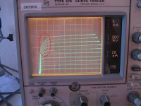
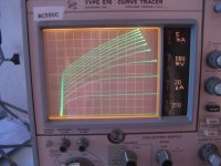
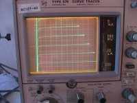
I just took I-V curves of 3 small signal NPN transistors (Thurs 01 Aug 2013, at 18:55 GMT). They are attached. I believe DIYaudio members call the phenomenon circled in red, by the name "quasi saturation". Device type is noted in the upper left. Sorry I didn't use a Polaroid scope camera
You'll see that all three measurements use the same setup:
You'll see that all three measurements use the same setup:
- 10 steps of base current @ 20 uA per step
- Vce = 0v to 5V @ 0.5V per division
- Ice = 5 mA per division, 10 vertical divisions max
Attachments
Last edited:
Thank you!! You have some decent equipment.
The phenomena is very real then. I best obtain a decent amount BC337-40s then.
If I'm understanding the pics right the BC337-40 looks almost ideal at low Vces.
Things are progressing. I have pieced together a BOM and placed orders for some components. Just finalising the last two orders. The PCBs should arrive sometime next week. Then its build time.
Changed to BC5xx devices where the transistors are subject to low Vce. This was prompted after reading about quasi saturation in the impressive astx thread.
Has the astx thread suddenly become unimpressive? Apparently it suggested that BC5xx transistors were preferred for low Vce applications; why reverse your decision so quckly?
Trust your gut; listen politely to the advice of strangers (definition: humans you don't know personally) and then make up your own mind. Remember that Satan constantly attempts to deceive you, from ever-changing directions. Remain wary.
The quasi-saturation curves don't seem to indicate Vbe modulation, which is just one low-Vce effect that happens to matter the most for my Kmultipliers. I wonder which manufacturer your BC550C came from? OnSemi and Fairchild are different. The same is true for the BC3x7.
Your curves will predict collector impedance at low Vce but will not predict Vbe modulation AFAIK. For instance I tried 2N3904 and it still had too much Vbe modulation. Your BC550C must be a different manufacturer because I've seen charts showing it to behave like the BC3x7.
If you switched the diamond collectors to the emitters of U27 and U28 it would be less of an issue. I know that Ib becomes Vce-dependent during quasi-saturation, so the BC3x7 should have more Ib linearity, so will distort less with significant source impedance.
The astx thread will always remain impressive especially the engineering at the end. Not changed my mind regarding devices just that the BC3x7-40 devices have now become an additional option for the diamond. The initial build will be as planned with the BC3x7 devices at the output and the BC5x0 devices elsewhere where low VCE is present. The 2n5401/2n5551 devices elsewhere.
As a side issue (not a US one), getting on semi BC3x7-40 devices means a mouser order only the Fairchild version seems to be easy to get from local suppliers. This isn't a problem just means moving one order to mouser to avoid shipping charges.
Ever changing directions... Yes I know about that one. It still happens now. Can end up going round in circles and getting nowhere. That's why I just decided enough was enough and ordered the PCBs. I got to a point where I thought I had a reasonable solution. The PCBs layouts do allow some easy mods to other possible ideas.
Linearity due to source impedance shouldn't be too much of an issue as these amps will be preceded in the chain by active crossovers which have yet to be designed. There will be by default some sort of buffer between the source and the amps.
It only works!!!!
Almost exactly as the simulation predicted.
The only small difference was the boot straps. They were predicted at +/-15V and reality is +/-13V. Not a problem. Bias was simulated at 150mA and is as close as damn it. Can't see any oscillation with the MOSFETs which was a relief.
Square waves with no overshoot but not as defined as the simulation.
Learnt that grounding is ABSOLUTELY critical. Got a bit of a noise problem getting in but that I think is the result of the test setup. Going to have to improve that. Once I sort the noise issue I'll post some pics.
It is stable into the test speaker without the L//R output filter. I have run at various levels and from frequencies 3Hz to 100kHz. Unloaded it gets to within 3V of the rails. It also clips nicely unloaded.
Where to go next is the question... Aside from the noise issue what is the next step?
Really pleased with initial testing especially for it being the first amp I have ever designed.
Paul
Congrats, it was to expect after all that hard work. After solving ground issues it is music enjoyment next. And never ending sound improvements of course. Components experimenting, you'll see. And maybe sharing to diy forum
...Congrats, it was to expect after all that hard work. After solving ground issues it is music enjoyment next. And never ending sound improvements of course. Components experimenting, you'll see. And maybe sharing to diy forum
Thank you. I will share do not worry. Lots of people have helped make this happen. Couldn't have done it by myself. The least I can do is share it once fully developed.
Thank you to all that have helped me in this quest, overall feedback, keanetoken, manso, andrewt, transistormarkj et al. (List in no particular order
)Your help is beyond computation.
Sorted out the noise issues. Just taped all the pairs of conductors together and the noise virtually dissappeared. Been giving the single channel a listen and in mono and off an mp3 player it sounds pretty good.
Looks like a very good job!
Also twist the pairs and the noise should almost disappear. (Of course, you should have done that before both ends were connected...)
By the way, what phase margin did you end up with, in simulation?
Take a look at pages 17-22 of this excellent PDF:
http://www.onsemi.com/pub_link/Collateral/TND352-D.PDF
Not sure how directly it applies, here. But it relates open-loop phase margin to closed-loop Q factor. A closed-loop Q of 0.5 is probably the ideal case, since it gives fast response with no overshoot. It corresponds to an open-loop phase margin of 76 degrees. But they also suggest designing for 70 degrees. They're not talking about an amplifier but the control-system stuff should be generally applicable.
Thank you for the link. yes it makes sense, an amplifier is just a control system at the end of the day.
I did plait the power leads but then got the grounding wrong and got some strange square wave oscillation. Then the path of least resistance was to use tape.
PM in simulation is 58 degrees. Gives enough stability to drive a speaker directly.
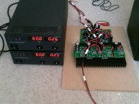
Here's a pic of the initial setup. It now has 2 pairs of outputs. And no oscillation!
I did plait the power leads but then got the grounding wrong and got some strange square wave oscillation. Then the path of least resistance was to use tape.
PM in simulation is 58 degrees. Gives enough stability to drive a speaker directly.
Here's a pic of the initial setup. It now has 2 pairs of outputs. And no oscillation!
Attachments
Looks like a very good job!
Also twist the pairs and the noise should almost disappear. (Of course, you should have done that before both ends were connected...)
By the way, what phase margin did you end up with, in simulation?
Take a look at pages 17-22 of this excellent PDF:
http://www.onsemi.com/pub_link/Collateral/TND352-D.PDF
Not sure how directly it applies, here. But it relates open-loop phase margin to closed-loop Q factor. A closed-loop Q of 0.5 is probably the ideal case, since it gives fast response with no overshoot. It corresponds to an open-loop phase margin of 76 degrees. But they also suggest designing for 70 degrees. They're not talking about an amplifier but the control-system stuff should be generally applicable.
Excellent pdf indeed

Most dont take the Q into consideration.The 76 degrees phase margin is about optimum, personally I find between 75 and 85 best for power amps.
- Status
- This old topic is closed. If you want to reopen this topic, contact a moderator using the "Report Post" button.
- Home
- Amplifiers
- Solid State
- Amp design attempt number 2 (simpler)