I see there is a panic in the forum for these 11.34 microseconds
...
So I would like to know if someone have found problem using headphone.
Not panic as "it does not hurt my purist ear, it hurts my purist eye".
With my AD1865 DAC and speakers no delay can be heard, and it is fare better of any my other sources.
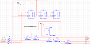
I looked through the I2S format (CS8414.pdf FMT2) and realized that is quite simple to make it EIAJ 18bit compatible:Will work on that one some time soon, if someone is keen to try and put out his/her ideas (in form of complete schematics), are also welcome to do this before me
The target would be:
Input: switchable in between 2 x true I2S 16 to 24 bit (not LSBJ or MSBJ)
Output: EIAJ 18bit (no delay)
1. Invert FSYNC
2. Shift FSYNC by 13clocks (32[word length] - 1[first tact] - 18[bit])
3[optional]. After this your shifter might be added for the sake of completeness
Sampler, could you simulate the above circuit to see the diagrams?
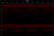
In the oscillogram from post #195 it's strange that Left Data is a continuous 1 while SDATA for Left Channel Word 01 is a sequence of 1010... Is there an error somewhere?
zsolt
I looked through the I2S format (CS8414.pdf FMT2) and realized that is quite simple to make it EIAJ 18bit compatible:
1. Invert FSYNC
2. Shift FSYNC by 13clocks (32[word length] - 1[first tact] - 18[bit])
3[optional]. After this your shifter might be added for the sake of completeness
Sampler, could you simulate the above circuit to see the diagrams?
In the oscillogram from post #195 it's strange that Left Data is a continuous 1 while SDATA for Left Channel Word 01 is a sequence of 1010... Is there an error somewhere?
zsolt
Ok, will do... as soon as I have some spare time.
No error there, because left word is sequence of 1111... (remember the relation to clock). Not the best solution for illustration purposes there, sorry.
When I was playing with AD1865, I was thinking about two options...
1) Use standard S/PDIF connection to CS8414 (18bit EIAJ). For CS/AD connection use only 1G logic just to invert LATCH for one chanel, nothing else.
2) Use output from CD player decoder (or PCM2707), in I2S or EIAJ format and shifter for DATA line to fit the AD1865 format.
I ended with second option. Only possible way was to use shifter, because AD1865 have only one clock pin, so stopped clock scheme (like with AD1861) is not possible here. Shifter was based on Rockna schematic, and there was relay for selecting input format (I2S/EIAJ16). DAC was working OK, with Sony (EIAJ16) and Philips (I2S) based CD players, and also with PCM2707 (I2S).
So if you have CS/AD connection, don't see any good reason for using shifter. If you want to connect AD1865 to CD player decoder chip without S/PDIF than Rockna shifter can be used.
Dear All,
I have assembled the DAC-END from Quanchao and Andrea. It works great !
Studying the documentation of the CS8414 I started playing with the status bits, and it looks like it shows the following error: bi-phase coding error .
Should it be like this ? What does it mean ?
D.
I have assembled the DAC-END from Quanchao and Andrea. It works great !
Studying the documentation of the CS8414 I started playing with the status bits, and it looks like it shows the following error: bi-phase coding error .
Should it be like this ? What does it mean ?
D.
As far as I'm concerned, beside the CS I want to connect the AD to an I2S device (probably a moded Squeezebox) and allow the selection between two I2S sources (selection done with simple relays).When I was playing with AD1865, I was thinking about two options...
1) Use standard S/PDIF connection to CS8414 (18bit EIAJ). For CS/AD connection use only 1G logic just to invert LATCH for one chanel, nothing else.
2) Use output from CD player decoder (or PCM2707), in I2S or EIAJ format and shifter for DATA line to fit the AD1865 format.
I ended with second option. Only possible way was to use shifter, because AD1865 have only one clock pin, so stopped clock scheme (like with AD1861) is not possible here. Shifter was based on Rockna schematic, and there was relay for selecting input format (I2S/EIAJ16). DAC was working OK, with Sony (EIAJ16) and Philips (I2S) based CD players, and also with PCM2707 (I2S).
So if you have CS/AD connection, don't see any good reason for using shifter. If you want to connect AD1865 to CD player decoder chip without S/PDIF than Rockna shifter can be used.
I plan to create a board which contains only the shift logic + AD + passive I/V and has two plugs for two I2S daughter boards. One board will contain the CS logic and the other will interface another I2S.
Zsolt
Some updates.
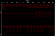
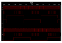
Source is 24bit I2S. Two versions, one shifting FSYNC by 19 CLK as proposed by vzs (not 13, as only 12 bits are latched in that case), and second "for purist eyes" shifting data properly for AD1865. Extra buffering was applied in both cases for signals that are not shifted to get everything in sync. In first version, only inverted LR is out of sync by HC02 propagation delay. In second version everything is in perfect sync, that is according to multisim of course")
There is a couple things that worries me. In both versions data is 24bit words. In first version each DAC channel gets leftovers from another one (6bits). That's maybe not the biggest problem, as 1865 transfers just "last 18 bits which were clocked into the Serial Registers to be shifted into the DACs". In second version, no such problem exists. Now the funny part. What happens when word is 16bit length ? Last 2 accuracy bits will always be 0 Is this the way it's supposed to be ? I'm wondering how this is implemented in such a receivers as CS8614. Outputting 18bit word from 16bit received data. Anyone care to explain ?
Source is 24bit I2S. Two versions, one shifting FSYNC by 19 CLK as proposed by vzs (not 13, as only 12 bits are latched in that case), and second "for purist eyes" shifting data properly for AD1865. Extra buffering was applied in both cases for signals that are not shifted to get everything in sync. In first version, only inverted LR is out of sync by HC02 propagation delay. In second version everything is in perfect sync, that is according to multisim of course
There is a couple things that worries me. In both versions data is 24bit words. In first version each DAC channel gets leftovers from another one (6bits). That's maybe not the biggest problem, as 1865 transfers just "last 18 bits which were clocked into the Serial Registers to be shifted into the DACs". In second version, no such problem exists. Now the funny part. What happens when word is 16bit length ? Last 2 accuracy bits will always be 0
Is this the way it's supposed to be ? I'm wondering how this is implemented in such a receivers as CS8614. Outputting 18bit word from 16bit received data. Anyone care to explain ?Attachments
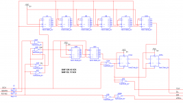
Now the funny part. What happens when word is 16bit length ? Last 2 accuracy bits will always be 0
Last two bits will be zero all the time. This is normal. It is working on this way with CS (18 bit EIAJ output mode) also.
@sampler
Very nice! would be interesting to try both on veroboard. In two weeks I will have my CS8414, and if I'm lucky and its not faulty (as most of them bought from tube_buyer are) I will try the first version. Probably I will try the Dac End2 solution first (one 74HC04) that is version 0
Are you using Multisim? If yes, I would be glad if you could send me the project files of these simulations. Thanks!
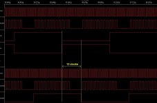
Actually I was referring to those 13 CLKs (see attachment). I'm still wondering why 32-13=19 CLKs has to be shifted... but I will figure out hopefully Today I'm a bit heavy-headed...
Very nice! would be interesting to try both on veroboard. In two weeks I will have my CS8414, and if I'm lucky and its not faulty (as most of them bought from tube_buyer are) I will try the first version. Probably I will try the Dac End2 solution first (one 74HC04) that is version 0
Are you using Multisim? If yes, I would be glad if you could send me the project files of these simulations. Thanks!
Actually I was referring to those 13 CLKs (see attachment). I'm still wondering why 32-13=19 CLKs has to be shifted... but I will figure out hopefully
Today I'm a bit heavy-headed...Attachments
Last edited:
Last two bits will be zero all the time. This is normal. It is working on this way with CS (18 bit EIAJ output mode) also.
Ok, so no problem there, thanks.
Are you using Multisim? If yes, I would be glad if you could send me the project files of these simulations. Thanks!
Yes, MS11. Here you go:
Free unlimited file hosting - Nemokama talpykla, failø talpinimas ir atsisiuntimas
Any hint on this ?
Dear All,
I have assembled the DAC-END from Quanchao and Andrea. It works great !
Studying the documentation of the CS8414 I started playing with the status bits, and it looks like it shows the following error: bi-phase coding error .
Should it be like this ? What does it mean ?
D.
Dear All,
I have assembled the DAC-END from Quanchao and Andrea. It works great !
Studying the documentation of the CS8414 I started playing with the status bits, and it looks like it shows the following error: bi-phase coding error .
Should it be like this ? What does it mean ?
D.
Any hint on this ?
Dear All,
I have assembled the DAC-END from Quanchao and Andrea. It works great !
Studying the documentation of the CS8414 I started playing with the status bits, and it looks like it shows the following error: bi-phase coding error .
Should it be like this ? What does it mean ?
D.
Somehow missed this point. I look at it when have board and scope at my hand reach. Maybe just random frame from your source was not 100% right. It's enough for 1 bad frame and this error would stay.
So I don't have to lose sleep about it ?
D.
Naaah... not worth it. As I mentioned, this means that internal PLL could lock onto your sampling rate and properly decode SPDIF frames, but at some point there was error in received bi-phase coded data (SPDIF frame has a lot more than just audio data). This error bit stays latched, until SEL leg is lifted to HIGH for eight mck cycles.
Is it possible modify the possitive regulator to give 3,3v for another projekt I am building?
Everything is possible, wrong thread tho...
http://www.diyaudio.com/forums/powe...listic-salas-low-voltage-shunt-regulator.html
- Status
- This old topic is closed. If you want to reopen this topic, contact a moderator using the "Report Post" button.
- Home
- Source & Line
- Digital Source
- AD1865 the best DAC