I'm going to build a symmetrical amplifier with minimum component (seems stupid) and I'm lack of knowledge (scratching from zero now), thus I name it 'Absolute Zero'.
(Just started to learn simulation too)
The aim of this amp is to let me understand (and some beginner too) by building amplifier beginning with only transistor (BJT now, maybe others later), then increase components that only 'necessary' to make the amplifier work sufficiently.
and the second stage is to make this amplifier sound nice and clean (improve the amplifier in short)
then maybe third stage is to make high power/performance, but we just make the first stage first.
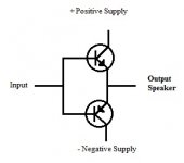
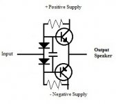
So here I attached the schematic I have drawn, with symmetrical output transistors only, each individual responsible for halfwave(AC positive and negative portion) of the audio input.
Welcome to add any component to make this amp work stable and safe FIRST, and state (briefly explain would be good) the reason/function of adding it. (each single component explanation would be best)
(Just started to learn simulation too)
The aim of this amp is to let me understand (and some beginner too) by building amplifier beginning with only transistor (BJT now, maybe others later), then increase components that only 'necessary' to make the amplifier work sufficiently.
and the second stage is to make this amplifier sound nice and clean (improve the amplifier in short)
then maybe third stage is to make high power/performance, but we just make the first stage first.
So here I attached the schematic I have drawn, with symmetrical output transistors only, each individual responsible for halfwave(AC positive and negative portion) of the audio input.
Welcome to add any component to make this amp work stable and safe FIRST, and state (briefly explain would be good) the reason/function of adding it. (each single component explanation would be best)
Attachments
I'll go first, for the s***s and grins. The one component I would add is a single-cell battery, in place of the connection from the input to the top transistor's base, with the positive connection to the base. An alkaline cell with 1.5V would be good for silicon transistors (which I presume these are), but it's possible for that to be a little too much bias voltage, causing excess idle current. A NICD or NIMH at 1.2 volts might work better as far as lower idle current, the tradeoff of course being greater crossover distortion, but still a substantial improvement over the original circuit.
I'm reminded of an Albert Einstein quote that something "should be as simple as possible, but no simpler."
I'm reminded of an Albert Einstein quote that something "should be as simple as possible, but no simpler."
I'm agree that quote, but my motive is not to make it THAT simple, but instead add on each component in order to make it work, the motive is to make me understand. (other tutorial or books I have seen always state the whole circuit as a start, already more than 5 component or so, thus couldn't understand what is the use of each component)I'll go first, for the s***s and grins. The one component I would add is a single-cell battery, in place of the connection from the input to the top transistor's base, with the positive connection to the base. An alkaline cell with 1.5V would be good for silicon transistors (which I presume these are), but it's possible for that to be a little too much bias voltage, causing excess idle current. A NICD or NIMH at 1.2 volts might work better as far as lower idle current, the tradeoff of course being greater crossover distortion, but still a substantial improvement over the original circuit.
I'm reminded of an Albert Einstein quote that something "should be as simple as possible, but no simpler."
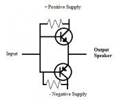
Hm... I also think of biasing for quiescent current, but how to achieve that ? (just putting resistor is fine ? as attached. seems easy to change Iq when temperature rise)
Attachments
The two bases are still shorted, so no bias current just wasting supply current. You must put something between the bases. Bare minimum is a resistor, but this will give you poor temperature stability. Better would be a pair of diodes, as these would roughly match the base-emitter voltage of the BJTs.
Do the diode also for thermal compensation (prevent thermal runaway) ?The two bases are still shorted, so no bias current just wasting supply current. You must put something between the bases. Bare minimum is a resistor, but this will give you poor temperature stability. Better would be a pair of diodes, as these would roughly match the base-emitter voltage of the BJTs.
Is it necessary to thermal couple the diode with output transistor ? like NJL3281 pair ?
Does the resistor I add there appropriate ?
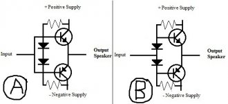
I have attached the redrawn diagram, adding 2 diodes there. (should it be thermally coupled like NJL3281 pair ?)
The direction of diode can be change ? or this is wrong setup (I have the feel of that)
(A) configuration seem no different, also shorting.
(B) configuration seem no shorting, but no signal conduction. (maybe should reverse the direction.
Additional question : Does the 'usual' amplifier have bias current go through to input/VAS driver transistor ?
Attachments
I am also very naive to the function of all the parts of an amplifier circuit. I have built a few kits, but to be quite honest I did not understand the function of each part. I think this is a great idea for a thread and I will be following it closely and I have my iron ready and my Radio Shack board ready to learn along with you.
B is correct. The signal will travel through the diodes, but you can also add capacitors in parallel with them. The diodes should be thermally coupled to the BJT.
The standard amplifier arrangement has output base bias current going through the VAS collector circuit. The output base voltage is set by a Vbe multiplier circuit, rather than a pair of diodes.
The standard amplifier arrangement has output base bias current going through the VAS collector circuit. The output base voltage is set by a Vbe multiplier circuit, rather than a pair of diodes.
Haha, thanks. I personally also build, repair, modding few amplifier, similar situation with you. I'm curious about what stage I would reach. (I'm learning simulation at the same time, multi-tasking i think)I am also very naive to the function of all the parts of an amplifier circuit. I have built a few kits, but to be quite honest I did not understand the function of each part. I think this is a great idea for a thread and I will be following it closely and I have my iron ready and my Radio Shack board ready to learn along with you.
If you saw anything that you doesn't understand,not sure, or not stated, please voice out (because maybe i would miss out something) since this is a total learning session
hm.... really ? it seems that positive halfwave 'should' go through the top transistor, but it seems the diode is in reverse bias, thus no positive signal allow to go there.B is correct. The signal will travel through the diodes, but you can also add capacitors in parallel with them. The diodes should be thermally coupled to the BJT.
The standard amplifier arrangement has output base bias current going through the VAS collector circuit. The output base voltage is set by a Vbe multiplier circuit, rather than a pair of diodes.
The opposite also same, the negative portion of signal can't go to the bottom transistor.
About the capacitor's function ? (block DC ?) why not we eliminate the diodes and put capacitor in between ? this will block biasing DC and allow signal to flow freely.
Based on your answer, i assume that Iq only apply to VAS and output transistor ?
I have attached another schematic, with also have (A) and (B).
(A) - Using Capacitor at value which allow AC signal to pass, but block bias DC.
(B) - Bias DC are block by diodes (reverse bias) and AC signal are allow to pass through diodes (forward bias)
Attachments
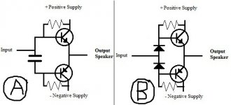
Your new A would work, with the output devices now receiving current bias rather than voltage bias.
Your new B would only provide any output with a big input signal, and would suffer from serious crossover distortion. Essentially, it would only respond to inputs with an amplitude greater that about 1.2-1.4V and would delete the central part of the waveform near the zero crossing.
I don't want to rain on your parade, but your questions suggest to me that you still have a lot of reading to do on fundamentals before you can design even an 'Absolute Zero' design. Putting up bad designs then asking people to point out the flaws in them is an inefficient way of learning the basics for both pupil and teacher!
I would absolutely recommend you spend some time studying Horowitz and Hill. Not only will you learn the basics that you need before trying to design something yourself, they have a cool pedagogical trick that's apropos here: at the end of every chapter, they show a set of "Bad Circuits" for the reader to diagnose. A circuit very much like yours appears at the end of one of the early chapters.
hm... I'm agree that sometimes this is a bad way to do, but I prefer to do both at the same times, since SY recommend some book, I will read through in the meantime, hope you will also help me.Your new A would work, with the output devices now receiving current bias rather than voltage bias.
Your new B would only provide any output with a big input signal, and would suffer from serious crossover distortion. Essentially, it would only respond to inputs with an amplitude greater that about 1.2-1.4V and would delete the central part of the waveform near the zero crossing.
I don't want to rain on your parade, but your questions suggest to me that you still have a lot of reading to do on fundamentals before you can design even an 'Absolute Zero' design. Putting up bad designs then asking people to point out the flaws in them is an inefficient way of learning the basics for both pupil and teacher!
Ok, since the newer B was not good, then just avoid it for now (until i understand whats happening).
About (A), what value should the capacitor be (roughly) ? I don't think alone would make the amplifier work safely, what could still be add in ?
SO I attached the previous diagram, with capacitor parallel to those diode, is it correct ? What is its purpose ?B is correct. The signal will travel through the diodes, but you can also add capacitors in parallel with them. The diodes should be thermally coupled to the BJT.
Thanks for suggesting those books, will look into those tomorrow.I would absolutely recommend you spend some time studying Horowitz and Hill. Not only will you learn the basics that you need before trying to design something yourself, they have a cool pedagogical trick that's apropos here: at the end of every chapter, they show a set of "Bad Circuits" for the reader to diagnose. A circuit very much like yours appears at the end of one of the early chapters.
Attachments
Old (B) already was quite close to what one might find as a buffer in a headphone amplifier. Only the emitter resistors are still missing, which are used to swamp part variances and counteract thermal runaway.
Here's a typical headphone amplifier circuit from about 25 years ago, "borrowed" from a Yamaha preamp.

This one was designed to competently drive line-level and mid- to high-impedance (~100...2k ohms) headphone loads, hence they could afford 33 ohm emitter resistors. I would use no larger than about 4.7 ohms today, otherwise open-loop gain into 16 ohms loads would suffer. Bias diode current is provided by the opamp here instead of having a second resistor, which should give better PSRR at this point.
Opamps are happiest when they don't have to drive too much current, as their output stages aren't exactly super beefy. Think no more than about 10 mA rms or so in this case. Hence a buffer will be appreciated especially if loads of far less than 600 ohms are connected.
The OP's homework will be reading up on transistor beta and gain-bandwidth product / fT, and then explaining why setups like these aren't normally used with speakers.
Here's a typical headphone amplifier circuit from about 25 years ago, "borrowed" from a Yamaha preamp.
This one was designed to competently drive line-level and mid- to high-impedance (~100...2k ohms) headphone loads, hence they could afford 33 ohm emitter resistors. I would use no larger than about 4.7 ohms today, otherwise open-loop gain into 16 ohms loads would suffer. Bias diode current is provided by the opamp here instead of having a second resistor, which should give better PSRR at this point.
Opamps are happiest when they don't have to drive too much current, as their output stages aren't exactly super beefy. Think no more than about 10 mA rms or so in this case. Hence a buffer will be appreciated especially if loads of far less than 600 ohms are connected.
The OP's homework will be reading up on transistor beta and gain-bandwidth product / fT, and then explaining why setups like these aren't normally used with speakers.
I think the OP still needs to read up on basic circuits. He is still quite a long way off worrying about bandwidth issues.
A capacitor across each diode would be better than one joining the bases. The cap value depends on lowest frequency to be amplified and diode dynamic impedance, which in turn depends on current. Current will be somewhat greater than BJT base current, but difficult to calculate due to production spreads.
H&H is one book with two authors.
You probably didn't learn to walk (=basic circuit design) by repeatedly falling off a bicycle (=thermally tracked push-pull design). At least, I didn't and I assume others do it the same way. Don't even think about a motorbike (=full amp with mains PSU)! Try to design a simple common-emitter BJT voltage amplifier, and understand what each component does and what its value should be. Build it and test it. Then you will be able to walk.
http://www.stanford.edu/class/ee122/Handouts/EE113_Course_Notes_Rev0.pdf
I find some of these first year EE course materials rather useful, and I was where you are not a long time ago.
You could always read up on headphone amplifier circuits, starting with resistor loaded single emitter follower, referencing back to how a NPN transistor looks just like a triode, and from there move to a class B stage that has significant crossover distortion, then learn about AB biasing, in which you overlap the transistor turn on times...etc
In the process of trying to learn all this without proper background, I found sites like tubecad, headwize, and of course diyaudio fairly useful, and google is always your friend
I'll throw out my own noob question:
CCDA & Class-AC
Has any one had experience with this so call "Corbeil Class B Auto Bias"?
I know there is prior art, and that perhaps I should not use Corbeil's name there, but for discussion's sake...
It looks fairly similar to the circuit from the Yamaha preamp, only that it's upside down, with the opamp providing bias from the bottom, and transistors instead of diodes.
The question is, how well does this work in reality?
http://www.edn.com/contents/images/6702272.pdf
Note in the EDN article this was published, there is an additional capacitor across the first transistor pair.
Would it be beneficial to add some emitter resistors to the output pair like it's done in a AB output stage?
From my understanding they should provide some local feedback to linearize the outputs transistors and provide some protection.
aw..... its really hard to design 'absoute zero', was studying 3 book at the same time (EE113, art of electronic, douglas self's amplifier book).
As douglas said its book, it seems that it was pointless to avoid 3 stages, minimum of 2 stages (but with very difficult to design). So should I start with simple 3 stages ? (transconductance, transadmittance, unity-gain buffer)
As douglas said its book, it seems that it was pointless to avoid 3 stages, minimum of 2 stages (but with very difficult to design). So should I start with simple 3 stages ? (transconductance, transadmittance, unity-gain buffer)
IMHO, learn about the three basic transistor building blocks, the Common Emitter, Common Collector, and Common Base. Be familiar with what other types of components do, what their characteristics are and how they are used, such as resistors, capacitors, inductors, diodes and the like. Then you will recognize where voltage gain is coming from, current gain (buffering) and other things like cascoding and current sources when you see them.
I think the main problem previously is that I don't know how the signal processed in transistors. (I only think them as electron flow from base to emitter or vice versa only)IMHO, learn about the three basic transistor building blocks, the Common Emitter, Common Collector, and Common Base. Be familiar with what other types of components do, what their characteristics are and how they are used, such as resistors, capacitors, inductors, diodes and the like. Then you will recognize where voltage gain is coming from, current gain (buffering) and other things like cascoding and current sources when you see them.
Limiting where output only at emitter (similar to common emitter), other components should be no problem.
I WAS just reading about cascode, gain buffer, etc...... seems I hit on the correct spot.
- Status
- This old topic is closed. If you want to reopen this topic, contact a moderator using the "Report Post" button.
- Home
- Amplifiers
- Solid State
- [Absolute Zero] Design Amp with minimum component (understanding too)