Here is an amplifier circuit that is as simple as I can think of right now that actually works.
It can be thought of as two halves, i.e. on both sides of the power supply (batteries) in the drawing.The left hand side, i.e. the opamp, amplifies the voltage. The right hand side amplifies the current. I used Darling transistors to keep it simple.
LTspice shows that the thing works, with 15W output power into 8 ohm with THD at 0,008% for a 1kHz input. Sadly, THD rises rapidly with frequency, reaching 0,4% at 20 kHz. The circuit has many other shortcomings but is presented in the hope that it will give some insight into how an amplifier works.
Attachments

Last edited:
Yeah, I had some overview, but the front end is Integrated Circuit in your example. (want to build full discrete one) But nevertheless its simple and niceHere is an amplifier circuit that is as simple as I can think of right now that actually works.
It can be thought of as two halves, i.e. on both sides of the power supply (batteries) in the drawing.The left hand side, i.e. the opamp, amplifies the voltage. The right hand side amplifies the current. I used Darling transistors to keep it simple.
LTspice shows that the thing works, with 15W output power into 8 ohm with THD at 0,008% for a 1kHz input. Sadly, THD rises rapidly with frequency, reaching 0,4% at 20 kHz. The circuit has many other shortcomings but is presented in the hope that it will give some insight into how an amplifier works.
I'm curious why is there 5 diode, is it necessity to have so much diodes ?
I can see that my previous design lack of emitter resistor, it is a necessity, but forgot why it is needed, anyone could help out ? (something like prevent direct connecting the output transistor)
The five diodes are there to bias the base-emitter junctions in the two Darlington transistors. There are four of them. The "on" voltage for the diodes are not quite same as that of the transistors, therefore an extra one is added to make sure that there is no crossover distortion.
As for those emitter resistors, they can in fact be left out. The circuit will work without them. Performance is degraded a little, but as we are trying to get away with the minimum number of components we can do that.
As for those emitter resistors, they can in fact be left out. The circuit will work without them. Performance is degraded a little, but as we are trying to get away with the minimum number of components we can do that.
Attachments

I'm looking at that R7 between the opamp output and the minus supply - it doesn't look needed to me. And the thing looks scary without the emitter resistors. They at least partly reduce the chance of thermal runaway in the output devices. Being darlingtons (two transistors in each case), both the driver's and output's Vbe's will drop as they heat up.
As for a textbook/tutorial, I've mentioned the ARRL Radio Amateur's Handbook before. Get any edition from the last 30 or 40 years, it goes from basic "these are resistors and capacitors" stuff to complicated stuff involving transistors and opamps in about 100 fast-paced pages. The Horowitz and Hill book, "The Art of Electronics," would then be Volume Two of electronics education.
As for a textbook/tutorial, I've mentioned the ARRL Radio Amateur's Handbook before. Get any edition from the last 30 or 40 years, it goes from basic "these are resistors and capacitors" stuff to complicated stuff involving transistors and opamps in about 100 fast-paced pages. The Horowitz and Hill book, "The Art of Electronics," would then be Volume Two of electronics education.

If you drive ground with this circuit and take the feedback from the center-tap on the transformer (QSC method) back to the input (with a series resistor to the input), you will have a complete amplifier.
"it doesn't look needed to me"
Most opamps can source current, but they can't sink it very well.
I would probably use an emitter resistor, and a base resistor too.
The diode string needs to be on the heatsink, and I would put a pot in parallel with one of those diodes.
*****************
On my idea, I would use a 2K input resistor, and a 20K dfeedback resistor. I would also include a pot to inject some current to the input summing node for a DC balance.
The cool follower 99 posted by djk, is very little component X.x and could be more simple with decreasing of parallel output into single output pairs.
Do you know any reason for resistor before going to the input pairs from power rails ? (0.18R) and 390R is for reduce voltage for input pairs and biasing output pairs ?
As what I saw, the input pairs doesn't have any bias current (correct if wrong), thus maybe the frequency response will be weak ?
I assume the input transistors are in common collector arrangement ?
(let's reduce the component to the minimum, then start to increase it)
For me, it looks simple and nice. !
Any reasons for capacitor between the outputs of input transistor ?
Extra : any thermal compensation device ? seems is prone to thermal runaway !
Last edited:
So the extra diode is 'extra' to ensure no crossover distortion.The five diodes are there to bias the base-emitter junctions in the two Darlington transistors. There are four of them. The "on" voltage for the diodes are not quite same as that of the transistors, therefore an extra one is added to make sure that there is no crossover distortion.
As for those emitter resistors, they can in fact be left out. The circuit will work without them. Performance is degraded a little, but as we are trying to get away with the minimum number of components we can do that.
What does the R6 do, which is nearby the output.
I'm agree that adding emitter resistor would be better, but it 'CAN' be removed, but less add it on ^^I'm looking at that R7 between the opamp output and the minus supply - it doesn't look needed to me. And the thing looks scary without the emitter resistors. They at least partly reduce the chance of thermal runaway in the output devices. Being darlingtons (two transistors in each case), both the driver's and output's Vbe's will drop as they heat up......
If you remove the R7, you also need to remove R5 above, if not will effect the symmetry performance ? (I still have no idea what are they doing, possibly bias, but not sure)
Adding a pot parallel to those diode for adjust DC offset or bias ? why not remove one of the diode, and place a pot in the middle of those diode (2 diode each side), thus making adjustment easy ? (i'm very unsure what am I talking about, just sixth sense)
"Do you know any reason for resistor before going to the input pairs from power rails ? (0.18R) and 390R is for reduce voltage for input pairs and biasing output pairs ?"
The bias for the outputs is determined by the voltage dropped across the input 0.18Ω resistors, the 390Ω resistors are passive current sources.
"As what I saw, the input pairs doesn't have any bias current (correct if wrong), thus maybe the frequency response will be weak ? "
See above.
"Any reasons for capacitor between the outputs of input transistor ? "
The circuit is a diamond buffer, but de-biased into class AB. The capacitor allows the amplifier to move smoothly from class A to class AB.
For a 50W amplifier one set of outputs may be enough, Andrea was using paralleled cheap low power parts. Consider something like the 1302/3281 pairs. The input transistors must be on the same heatsink as the outputs.
"What does the R6 do, which is nearby the output."
It's the load (loudspeaker).
Last edited:
By the way, while Andea thought his cool follower was a new idea, if you take a look at the October 1976 Wireless World page 74, you will find the first amp of this type (that I am aware of).
Can't quite see how the input and output are biased through 0.18R, mind explaining ?The bias for the outputs is determined by the voltage dropped across the input 0.18Ω resistors, the 390Ω resistors are passive current sources.
The circuit is a diamond buffer, but de-biased into class AB. The capacitor allows the amplifier to move smoothly from class A to class AB.
For a 50W amplifier one set of outputs may be enough, Andrea was using paralleled cheap low power parts. Consider something like the 1302/3281 pairs. The input transistors must be on the same heatsink as the outputs.
"What does the R6 do, which is nearby the output."
It's the load (loudspeaker).
What is diamond buffer ? you mean the op amp or the whole circuit ?my only possible understanding is that biasing current is from power supply to top input transistor's emitter then base, then from bottom input transistor's base to emitter, then to negative rail. Then the bias current amplified is gone through output's base.
I definitely use 3281/1302, 0302/0281, 4281/4302 pairs.... i love them !
As what i saw, there is already a "out" terminal/node there, so why is the R6 still a load/speaker ? (or just because of simulation purpose ? )
Although it seems weird to ask here, but I still going to ask anyway.
By using the simplest form of BJT arrangement (common-emitter/base/collector), I have simulated using a JAVA applet.
But the results are unexpected, can anyway explain to me ?
The top circuit is a common-base, then common-collector, followed by common-emitter. all using NPN BJT
And the simulation (wave viewer) show in this order :
Input generator
Common-base circuit's 4ohm load
Common-collector circuit's 4ohm load
Common-emitter circuit's 4ohm load
Only common-collector's circuit seems normal for audio usage ? (trapped inside the mist !) according to the book/web, only common-emitter circuit should invert the signal, but seems different than saying... (common-collector's signal is inverted)
Attachments

One extra thing found out is although the common-collector have nice sine wave, but the voltage and current is way too small. (in pico)Only common-collector's circuit seems normal for audio usage ? (trapped inside the mist !) according to the book/web, only common-emitter circuit should invert the signal, but seems different than saying... (common-collector's signal is inverted)
I found out that the Rc and Re of respective circuit need to be tweak, but only differnet in output signal is common-base arrangement, which makes the circuit have making only halfwave, but it only have 5v, which is same as input.
Increase resistance also help common-base&emitter from shorting power supply.
By changing their gain, there are no difference except for common-emitter arrangement.
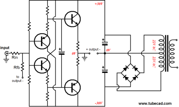
er.... the schematic seems weird ? The 0V is before and after the output (between 2 output emitter resistor), then how it is going to work ? (no output to output load)
and Rfb should be connected to output + ? and another resistor from output + to ground for controlling feedback ? (as voltage divider with Rfb)
I assume the input pairs and output pairs are common collector ?
and Rfb should be connected to output + ? and another resistor from output + to ground for controlling feedback ? (as voltage divider with Rfb)
I assume the input pairs and output pairs are common collector ?
"er.... the schematic seems weird ? The 0V is before and after the output (between 2 output emitter resistor), then how it is going to work ? (no output to output load)"
I'm sorry you can't understand the schematic. Most QSC, Hafler Transnova, one half side of Crown bridge amps, etc, are built this way.
"and Rfb should be connected to output + ? "
Of course not, how would it work? With the input wired as an inverving amplifier
"take the feedback from the center-tap on the transformer (post #25)"
"I assume the input pairs and output pairs are common collector ? "
Meaningless terms to me, I'd rather say 'emitter follower'.
It seems I overlook something. (try to understand) The ground is not 0V (in that schematic, ground is only connect between output+ to input ground.
Is seems if I include that point, everything seems workable, although not thoroughly understand. Such as how feedback in here works, and capacitor's usage.
Is seems if I include that point, everything seems workable, although not thoroughly understand. Such as how feedback in here works, and capacitor's usage.
By using the simplest form of BJT arrangement (common-emitter/base/collector), I have simulated using a JAVA applet.
Get LTspice, it's free. 😀
The picture you posted is a little hard to understand. 😕
x2Get LTspice, it's free. 😀
And join the corresponding Yahoo! group for more parts and stuff.
A diamond buffer wired "inside out" isn't exactly trivial to me (and I've been dabbling in circuits for a while), I imagine it would confuse the heck out of a n00b - well, it did. Not a terribly big fan of the diamond buffer so far. It is an inherently stable affair but seems to take lots of current for decent performance.
- Status
- Not open for further replies.
- Home
- Amplifiers
- Solid State
- [Absolute Zero] Design Amp with minimum component (understanding too)