agdr,
I PM'd u...please count me in for one board...
Alex
:>)
;
Hello Alex! I've added you to the order interest list out at the Google Drive link. I'll shoot a PM your way.
MUSES8820 chip for pre-amp
I've just decided to give something a try. For the (optional to populate) pre-amp chip on the ODA I've had the surface mount version of the LME49720 specified in the BOM. Remember that there are several ways that pre-amp out RCA jack can be wired, in the build instructions, all the way from wired stright through from the rear RCA input (or front 3.5mm jack input) to unity gain buffer with the chip or some voltage gain with the chip.
But I've recently discovered that Mouser now stocks the NJM "muses" supposedly high-end audio chips. The DIP versions are insanely expensive ($75 each or so at Mouser) but their "mass market" surface mount MUSES8820E bipolar chip goes for $10.
MUSES8820E NJR | Mouser
http://www.mouser.com/ds/2/294/MUSES8820_E-259018.pdf (opens PDF)
http://semicon.njr.co.jp/eng/MUSES/MUSES8820.html
When I build up my first ODA V2.0 I'm going to try the muses chip in for the pre-amp. Same pinout as the LME49720 so either chip would work. I've just been curious about the MUSES chips for awhile. This would fit right in with NwAvGuy's use of NJM chips in the O2. The MUSES line is supposed to be their top of the line audio chips, per the marketing materials.
There is nothing in the MUSES data sheet that really jumps right out, certainly nothing that would support $75 a chip. The data sheet specs for the LME49990 chips in the ODA gain stage exceed the muses line in all areas. The MUSES marketing materials have been a little cringe-worthy too which isn't garnering the chips much love, see this thread in the solid state forum:
http://www.diyaudio.com/forums/solid-state/223200-has-anyone-ever-had-experience-muse-opamps.html
Like I posteded in that thread the $850 Teac HA-501 headamp is using the MUSES8820 chip. Scroll down on that first page:
HA-501 | TEAC
That amp's variable damping factor switch is what I based the ODA's optional external rotary damping factor switch on.
Anyway this is all purely optional, the LME49720 fits in just fine for the pre-amp chp, and none of this has any effect on the main signal path in the ODA. I'll just be mighty curious to hear the results on the pre-amp out.
I've just decided to give something a try.
For the (optional to populate) pre-amp chip on the ODA I've had the surface mount version of the LME49720 specified in the BOM. Remember that there are several ways that pre-amp out RCA jack can be wired, in the build instructions, all the way from wired stright through from the rear RCA input (or front 3.5mm jack input) to unity gain buffer with the chip or some voltage gain with the chip.But I've recently discovered that Mouser now stocks the NJM "muses" supposedly high-end audio chips. The DIP versions are insanely expensive ($75 each or so at Mouser) but their "mass market" surface mount MUSES8820E bipolar chip goes for $10.
MUSES8820E NJR | Mouser
http://www.mouser.com/ds/2/294/MUSES8820_E-259018.pdf (opens PDF)
http://semicon.njr.co.jp/eng/MUSES/MUSES8820.html
When I build up my first ODA V2.0 I'm going to try the muses chip in for the pre-amp. Same pinout as the LME49720 so either chip would work. I've just been curious about the MUSES chips for awhile. This would fit right in with NwAvGuy's use of NJM chips in the O2.
The MUSES line is supposed to be their top of the line audio chips, per the marketing materials.There is nothing in the MUSES data sheet that really jumps right out, certainly nothing that would support $75 a chip. The data sheet specs for the LME49990 chips in the ODA gain stage exceed the muses line in all areas. The MUSES marketing materials have been a little cringe-worthy too which isn't garnering the chips much love, see this thread in the solid state forum:
http://www.diyaudio.com/forums/solid-state/223200-has-anyone-ever-had-experience-muse-opamps.html
Like I posteded in that thread the $850 Teac HA-501 headamp is using the MUSES8820 chip. Scroll down on that first page:
HA-501 | TEAC
That amp's variable damping factor switch is what I based the ODA's optional external rotary damping factor switch on.
Anyway this is all purely optional, the LME49720 fits in just fine for the pre-amp chp, and none of this has any effect on the main signal path in the ODA.
I'll just be mighty curious to hear the results on the pre-amp out.
Last edited:
Count me in for a couple of boards too mate!
Will do! I've added you to the list at the Google Drive ODA V2.0 link. You get the final two boards in this run.
I'll do a larger run after this one in a few weeks. I'll also be posting the Gerbers once the boards are back if anyone wants to run some of their own. Seeed Studio still has a 5 board minimum. Not sure what the minimums are for OSH park.
I'll take two on your next run>
Good deal. I've created a new list at the Google Drive link "next board run" and added you. You will also be first up if anyone from this run cancels.
If anyone else is interested in the next board run just go ahead an post on my vendor thread here
http://www.diyaudio.com/forums/vendors-bazaar/237226-parallel-njm4556al-two-stage-amp.html
or send me a PM and I'll add you to the list. Anyone can cancel of course, this just helps me to know about how many to have fabricated next time. Still the at-cost price of $15 a board plus shipping.
Put me down for four (4) ODA Version 2.0 PCB's
Put me down for four (4) ODA Version 2.0 PCB's. Is it possible to add, to this
future group buy, that soldering of the surface mount items to each of the PCB's?
I'm not very good at this so any help would be great. Take care.
Put me down for four (4) ODA Version 2.0 PCB's. Is it possible to add, to this
future group buy, that soldering of the surface mount items to each of the PCB's?
I'm not very good at this so any help would be great. Take care.
Put me down for four (4) ODA Version 2.0 PCB's. Is it possible to add, to this
future group buy, that soldering of the surface mount items to each of the PCB's?
I'm not very good at this so any help would be great. Take care.
Will do! I'll update the list. Thanks for your interest in the project. I'll send you a PM about the surface mount stuff.
Please put me down for 1x in the next batch. ThanksWill do! I'll update the list. Thanks for your interest in the project. I'll send you a PM about the surface mount stuff.
Please put me down for 1x in the next batch. Thanks
You are added.
I've forgotten to say that the boards will include the twelve 0.5R 1/8W balancing resistors for the output chips since neither Mouser or Digikey has 0.5R in 1/8W. The 1/4W I have as an alternate in the BOM works, but the 1/8W fit the best - and are all that is needed electrically.
Update...
Here is an update on a few things with this project.
The boards are finished and putting on some frequent flyer miles from China to the US. Looks like they are in customs right now from the tracking. With any luck I should get them this week and start building up one and testing it.
I've just posted a BOM and part ID diagram out at the Google Drive link for V2.0. The part ID diagram is the same kind of thing I did with the O2 booster board. Just a copy of the layout with a red circle around each part and its text part ID on the board, which should make it clearer which ID goes with which part in some of the denser sections of the board.
The BOM may change slightly when I start testing, so I would advise holding off buying parts if you are outside the US and are looking at a larger shipping cost with Mouser. So far the parts I've found that are out of stock at Mouser are the 1K audio pot and the input 3.5mm jack with the internal switch (Mouser has all on order though). Luckily Digikey has a big stock of both and I'll have a bunch here at-cost if anyone wants one with the board. In general it looks like Mouser has had a slight across the board price increase since I did the BOM last year. I've updated the parts prices in the BOM.
Mouser doesn't stock the two Linear Technology LDO regulators at all (or any LT parts for that matter), but Digikey does - or at least they are supposed to. Digikey is out of stock of the LT1963a, but Arrow has a bunch. I'll also have both those chips available at-cost too if anyone wants to avoid the separate orders.
And just a reminder of another cool modification you can do with the board, something I believe Sergey888 may have mentioned earlier in the thread. You can bump the input impedance up from 10K to 50K by simply replacing the two 10K input resistors with 50K and using LME49880 FET-input chips in place of the two LME49990 bipoar-input gain chips. The voltage noise is slightly higher with the LME49880, but you are going to get at bit of that anyway from increased Johnson noise if you have a larger source impedance, plus the current noise will be less and will counter-balance to some extent. The LME49880 is still rated for a 600 ohm load, so the 1K pot isn't a problem, and is still rated for the +/-16Vdc supply rails.
One more new bit of info I just learned about the front & back panels. I've done a first pass at the panels in Front Panel Express' CAD software as promised. In the process I've discovered the outfit I've been using, Proto Panel, appears to have stopped making front panels as of March 1. It would be nice to have an alternate to FPE given they cost about 2x what Proto Panel did, so I have an email into another outfit. Keep in mind too that the B4-080 case comes with blank front and back panels that can be drilled. I'll post all the hole measurements again in case someone has their own drill press and wants to give it a go.
I see that FPE allows sending in customer's own blank panels to use, but they only knock off about 8% of the cost for that, which would pretty much equal the cost of mailing the blank panels to them in the first place. There still might be a good reason to do that though. The edges on the panels from Proto Panel were not anodized blue since they milled the panels down from already-anodized stock. Presumably if you send the panels from the B4 box into FPE the blue anodization alreasdy on the edges will remain. I'll check on that with FPE.
I see that Allied Electronics has a couple of greeen and red B4-080's cases in stock along with a pile of black ones if anyone is interested in those colors. Newark also has the natural silver in stock. There is supposed to be a gold that isn't in stock anywhere, but I think it is possible to order single cases directly from Box Enclosures too.
Here is an update on a few things with this project.
The boards are finished and putting on some frequent flyer miles from China to the US. Looks like they are in customs right now from the tracking. With any luck I should get them this week and start building up one and testing it.
I've just posted a BOM and part ID diagram out at the Google Drive link for V2.0. The part ID diagram is the same kind of thing I did with the O2 booster board. Just a copy of the layout with a red circle around each part and its text part ID on the board, which should make it clearer which ID goes with which part in some of the denser sections of the board.
The BOM may change slightly when I start testing, so I would advise holding off buying parts if you are outside the US and are looking at a larger shipping cost with Mouser. So far the parts I've found that are out of stock at Mouser are the 1K audio pot and the input 3.5mm jack with the internal switch (Mouser has all on order though). Luckily Digikey has a big stock of both and I'll have a bunch here at-cost if anyone wants one with the board. In general it looks like Mouser has had a slight across the board price increase since I did the BOM last year. I've updated the parts prices in the BOM.
Mouser doesn't stock the two Linear Technology LDO regulators at all (or any LT parts for that matter), but Digikey does - or at least they are supposed to. Digikey is out of stock of the LT1963a, but Arrow has a bunch. I'll also have both those chips available at-cost too if anyone wants to avoid the separate orders.
And just a reminder of another cool modification you can do with the board, something I believe Sergey888 may have mentioned earlier in the thread. You can bump the input impedance up from 10K to 50K by simply replacing the two 10K input resistors with 50K and using LME49880 FET-input chips in place of the two LME49990 bipoar-input gain chips. The voltage noise is slightly higher with the LME49880, but you are going to get at bit of that anyway from increased Johnson noise if you have a larger source impedance, plus the current noise will be less and will counter-balance to some extent. The LME49880 is still rated for a 600 ohm load, so the 1K pot isn't a problem, and is still rated for the +/-16Vdc supply rails.
One more new bit of info I just learned about the front & back panels. I've done a first pass at the panels in Front Panel Express' CAD software as promised. In the process I've discovered the outfit I've been using, Proto Panel, appears to have stopped making front panels as of March 1. It would be nice to have an alternate to FPE given they cost about 2x what Proto Panel did, so I have an email into another outfit. Keep in mind too that the B4-080 case comes with blank front and back panels that can be drilled. I'll post all the hole measurements again in case someone has their own drill press and wants to give it a go.
I see that FPE allows sending in customer's own blank panels to use, but they only knock off about 8% of the cost for that, which would pretty much equal the cost of mailing the blank panels to them in the first place. There still might be a good reason to do that though. The edges on the panels from Proto Panel were not anodized blue since they milled the panels down from already-anodized stock. Presumably if you send the panels from the B4 box into FPE the blue anodization alreasdy on the edges will remain. I'll check on that with FPE.
I see that Allied Electronics has a couple of greeen and red B4-080's cases in stock along with a pile of black ones if anyone is interested in those colors.
Newark also has the natural silver in stock. There is supposed to be a gold that isn't in stock anywhere, but I think it is possible to order single cases directly from Box Enclosures too.
Last edited:
"Mouser doesn't stock the two Linear Technology LDO regulators at all (or any LT parts for that matter), but Digikey does - or at least they are supposed to. Digikey is out of stock of the LT1963a, but Arrow has a bunch. I'll also have both those chips available at-cost too if anyone wants to avoid the separate orders."
Yes please, I'll take LDO regs for 3 boards + panels for 3 boxes
Regards
Yes please, I'll take LDO regs for 3 boards + panels for 3 boxes
Regards
Yes please, I'll take LDO regs for 3 boards + panels for 3 boxes
Sounds good.
Once I get the boards back and tested I'll post a list of stuff available in the vendor forum thread. I'll send out PMs to let everyone know.
Last edited:
Regarding the front and back panels. I noticed on this O2 build blog, that the panels were made by https://www.ponoko.com/
I use my O2 exclusively on my desktop and would be happier with line out in addition to headphone out and a bass boost option. (The features of this ODA)
I am brand new here, but would it be possible to add me to the PCB order list?
I use my O2 exclusively on my desktop and would be happier with line out in addition to headphone out and a bass boost option. (The features of this ODA)
I am brand new here, but would it be possible to add me to the PCB order list?
Regarding the front and back panels. I noticed on this O2 build blog, that the panels were made by https://www.ponoko.com/
I use my O2 exclusively on my desktop and would be happier with line out in addition to headphone out and a bass boost option. (The features of this ODA)
I am brand new here, but would it be possible to add me to the PCB order list?
Hey thank you for the pointer to ponoko! I'll look into them. I also ran into another one today, emachineshop.com.
I'll add you to the list for the next board run. There is no commitment of any kind on the lists, anyone can cancel at any time, just helps me get a rough idea of how many boards to fab. Thanks for your interest in the project.

In pondering what NwAvGuy might have put in his ODA I added several things that people had posted about wanting in his blog comments, like the RCA jacks and power plug in the back. Then a bunch of things that just wouldn't fit in the O2 form factor and/or have too much current draw for batteries, but wouldn't be a problem in a desktop unit. The 2 stage pre-reg/LDO-reg power supply heat sinked to the back panel is a good example. No way to fit that into the O2's B2-080 box! Same with the rear RCA input jack and input select switch, or the 10 capacitors needed to maintain the O2's same low end corner frequency with the lower Johnson noise 1K pot and 4.99K ground return resistors.
Last edited:
Overlapping text IDs on the Part ID diagram
I forgot to say that in the Part ID diagram there are a few areas where it looks like a couple of part text labels are sitting right on top of each other. That is just one label for a part on the top of the board and the other on the bottom. On the layout diagram all the layers show up at once. The text for the parts on the bottom of the board shows up as mirrored from the top.
I forgot to say that in the Part ID diagram there are a few areas where it looks like a couple of part text labels are sitting right on top of each other. That is just one label for a part on the top of the board and the other on the bottom.
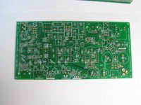
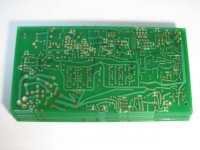
On the layout diagram all the layers show up at once. The text for the parts on the bottom of the board shows up as mirrored from the top.PC boards are in!
The boards for this project arrived today. Now to do some building and testing.
Photos:
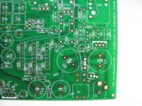
* The first two are the front and back of the boards. I do like how that ENIG (gold) finish turned out.
* The next two photos are a closeup of the AC power input & relay section, which is the first thing I'm going to build up and test. I've had suggestions from the folks who built the previous version for a more detailed set of build pictures. I'm going to take a bunch of photos of each section's build-up and post those out on the Google Drive link. I'm going to post this first bunch here since it shows some SMD soldering techniques and general build techniques. The revised build instructions will call the parts out by number for each section being built.
* The next two photos show how the SMD parts are packed from Mouser, for those builders who haven't messed with surface mount parts before. There is just a thin strip of plastic over the little cups that hold each part. Grab that strip at one end and peel it off over however many parts you want from the strip. Then flip the strip over and dump the parts out onto the PC board. In this case these are the 4 super-large (for SMD) 0.51 ohm 2W CRC resistors that go on the bottom of the PC board.
* Right off the bat I've discovered the first board error. I managed to get the text labels for two of the four 0.51R 2W resistors on the wrong side (top) of the board, R20 and R21. You can see the labels missing in the photo. Doesn't affect the circuit in any way, just the label. I'm going to start a list of any small board errata like this and post out on the Google Drive link.
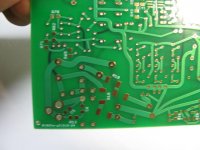
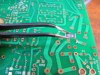
* The next four photos show how you go about soldering any of the two legged SMD parts on the board. First put a little solder on one of the two pads. Then grab the part by the sides with tweezers (right angle anti-static tweezers like these highly recommended). Then heat up that solder blob and stick an end of the part right into the solder, moving the part around as needed to line up the other pads. On a couple of the parts I had to re-heat that end one or more times to move the part around some more to get the part lined up the best on both pads. Try to line the part up so that at least a tiny amount of the other pad can be seen sticking out past the other end of the part. Once the solder on that end is cool and solid (give it at least 30 seconds to cool) go solder the remaining end. Then finally once that is cool (another 30 seconds) go back and touch up the first end with a little more solder and heat - if needed. And that is all there is to it!
Don't worry about that goopy looking flux residue at this point. That should get washed off down the road with some spray flux remover and a canned PC air duster.
Also note that resistors and capacitors are not static sensitive, nor are the particular diodes used in the power supply section, so I haven't bothered with setting things on an grounded anti-static mat or wear a grounded wrist strap at this point. Out of the entire power supply and relay section the only part that is static sensitive is the two 2N7000 mosfets for the relay. So I waited until last to put those in with all the anti-static stuff. It is always best to build up the circuit around static sensitive parts first so that there will be a load (to help dissipate static) on as many pins as possible after the part is soldered in.
The boards for this project arrived today. Now to do some building and testing.
Photos:
* The first two are the front and back of the boards. I do like how that ENIG (gold) finish turned out.
* The next two photos are a closeup of the AC power input & relay section, which is the first thing I'm going to build up and test. I've had suggestions from the folks who built the previous version for a more detailed set of build pictures. I'm going to take a bunch of photos of each section's build-up and post those out on the Google Drive link. I'm going to post this first bunch here since it shows some SMD soldering techniques and general build techniques. The revised build instructions will call the parts out by number for each section being built.
* The next two photos show how the SMD parts are packed from Mouser, for those builders who haven't messed with surface mount parts before. There is just a thin strip of plastic over the little cups that hold each part. Grab that strip at one end and peel it off over however many parts you want from the strip. Then flip the strip over and dump the parts out onto the PC board. In this case these are the 4 super-large (for SMD) 0.51 ohm 2W CRC resistors that go on the bottom of the PC board.
* Right off the bat I've discovered the first board error.
I managed to get the text labels for two of the four 0.51R 2W resistors on the wrong side (top) of the board, R20 and R21. You can see the labels missing in the photo. Doesn't affect the circuit in any way, just the label. I'm going to start a list of any small board errata like this and post out on the Google Drive link. * The next four photos show how you go about soldering any of the two legged SMD parts on the board. First put a little solder on one of the two pads. Then grab the part by the sides with tweezers (right angle anti-static tweezers like these highly recommended). Then heat up that solder blob and stick an end of the part right into the solder, moving the part around as needed to line up the other pads. On a couple of the parts I had to re-heat that end one or more times to move the part around some more to get the part lined up the best on both pads. Try to line the part up so that at least a tiny amount of the other pad can be seen sticking out past the other end of the part. Once the solder on that end is cool and solid (give it at least 30 seconds to cool) go solder the remaining end. Then finally once that is cool (another 30 seconds) go back and touch up the first end with a little more solder and heat - if needed. And that is all there is to it!
Don't worry about that goopy looking flux residue at this point. That should get washed off down the road with some spray flux remover and a canned PC air duster.
Also note that resistors and capacitors are not static sensitive, nor are the particular diodes used in the power supply section, so I haven't bothered with setting things on an grounded anti-static mat or wear a grounded wrist strap at this point. Out of the entire power supply and relay section the only part that is static sensitive is the two 2N7000 mosfets for the relay. So I waited until last to put those in with all the anti-static stuff. It is always best to build up the circuit around static sensitive parts first so that there will be a load (to help dissipate static) on as many pins as possible after the part is soldered in.
Attachments
-
 IMG_2396.JPG56.6 KB · Views: 425
 -
 IMG_2397.JPG54.4 KB · Views: 420
 -
 IMG_2398.JPG79.1 KB · Views: 415
 -
 IMG_2399.JPG57.8 KB · Views: 348
 -
 IMG_2400.JPG67.7 KB · Views: 353
 -
 IMG_2402.JPG48.6 KB · Views: 103
 -
 IMG_2406.JPG47 KB · Views: 111
 -
 IMG_2405.JPG52.2 KB · Views: 110
 -
 IMG_2404.JPG69.8 KB · Views: 115
 -
 IMG_2403.JPG43.1 KB · Views: 96
Last edited:
Power and relay section build photos, part 2
Continuing on...
* The first photo shows the more typical sized SMD part used on the board, a 1206 sized resistor for the snubber section. Same thing as with the 0.51R resistors, just a thin peel strip of plastic over the parts. Peel and dump. Then the same soldering procedure, just smaller.
* The next photo shows all the surface mount parts in the power supply & relay section, on the bottom of the PC board, soldered on now. In this section surface mounts parts are only on the bottom of the PC board, with all through-hole parts on the top.
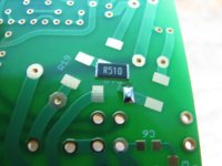
* The next two photos show how to "tombstone" or "end mount" a part. Several of the parts on the PC board are mounted like this to save space. You can see the particular symbol for that in the photo. One end had a circle around the hole to show the body of the part goes there, with the "flying lead" going in the other hole. Bend the flying lead first, as in the photo, then stick them both in and solder.
On all the through hole parts it is helpful to bend the leads on the back of the PC board just slightly, like 30 degrees or so, to hold the part in place when you flip the PC board over to solder. Then be sure to only solder one of the two part leads first, then flip the board over and see if the part is still against the board and straight up and down. If not put a little thumb pressure on it while you re-heat the solder on that lead to let the part drop down to the PC board. Then when it is position go solder the remaining lead on the part. You may want to go back to the first lead then and re-heat if needed for a second or two to get a nice joint.
Also notice that for "tombstoned" parts that have a polarity I've put some wording to show direction. Like for D16 here it says "band down" to be sure to put the banded end of that zener diode down toward that hole. The D15 1N4004 diode is labeled the same way. But the tombstoned R70 1W resistor in that photo doesn't have a polarity. No polarity marking and either end down is OK.
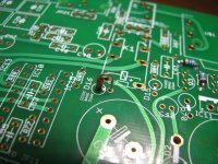
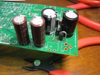
* The next photo shows the main rectifier diodes and electrolytic filter capacitors in place. You can also see that "tombstoned" R70 resistor installed now behind D2. It is a lot easier to solder the "interior" parts like this before the switch and power jack are installed. More room to work.
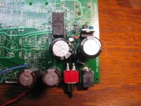
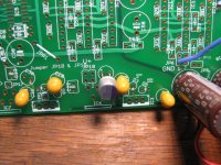
* The final two photos show all the power supply and relay parts installed. I've sprayed the section down with flux remover here too on the PCB underside. The wires I added for testing. Blue goes to ground (JP6), red to the V+ from the CRC section (JP8) and black to V- (JP9). I'll post a bunch of photos at the Google Drive link of the DC voltage testing with DMMs and scope shots of the output waveform under load.
Also remember there is a third voltage now, the +48Vdc voltage regulator powering the relay circuit. That is the T0-220 part sticking up in the photo, IC11 (TL783). The 48V regulator doesn't dissipate anywhere near enough heat to require heatsinking. The regulator is referenced to the negative power rail and not ground. To measure it measure from the lead of C50 nearest to the regulator to the V- negative power rail. Measuring it to ground will only yield half the voltage, 24V. You can hear the relay click when it engages. To test that just flip on the power switch and wait 5 seconds for the click!
In the photos I've also installed the R84 and R85 2.49k minimum output load resistors, even though they are not part of the power supply or relay section, just because R84 gets a little buried with the taller parts around it. Easier to install it now.
The top two leads coming out of the power switch get cut off, as in the photo (use wire cutters, those heavy leads will nick flush cutters). Turns out that DPDT switches are much more common than DPST, and the pricing is the same even when they are in stock, so it was easiest to use a DPDT and cut off two of the legs. I didn't run those two unused legs down to the PC board to save board space.
Continuing on...
* The first photo shows the more typical sized SMD part used on the board, a 1206 sized resistor for the snubber section. Same thing as with the 0.51R resistors, just a thin peel strip of plastic over the parts. Peel and dump.
Then the same soldering procedure, just smaller.* The next photo shows all the surface mount parts in the power supply & relay section, on the bottom of the PC board, soldered on now. In this section surface mounts parts are only on the bottom of the PC board, with all through-hole parts on the top.
* The next two photos show how to "tombstone" or "end mount" a part. Several of the parts on the PC board are mounted like this to save space. You can see the particular symbol for that in the photo. One end had a circle around the hole to show the body of the part goes there, with the "flying lead" going in the other hole. Bend the flying lead first, as in the photo, then stick them both in and solder.
On all the through hole parts it is helpful to bend the leads on the back of the PC board just slightly, like 30 degrees or so, to hold the part in place when you flip the PC board over to solder. Then be sure to only solder one of the two part leads first, then flip the board over and see if the part is still against the board and straight up and down. If not put a little thumb pressure on it while you re-heat the solder on that lead to let the part drop down to the PC board. Then when it is position go solder the remaining lead on the part. You may want to go back to the first lead then and re-heat if needed for a second or two to get a nice joint.
Also notice that for "tombstoned" parts that have a polarity I've put some wording to show direction. Like for D16 here it says "band down" to be sure to put the banded end of that zener diode down toward that hole. The D15 1N4004 diode is labeled the same way. But the tombstoned R70 1W resistor in that photo doesn't have a polarity. No polarity marking and either end down is OK.
* The next photo shows the main rectifier diodes and electrolytic filter capacitors in place. You can also see that "tombstoned" R70 resistor installed now behind D2. It is a lot easier to solder the "interior" parts like this before the switch and power jack are installed. More room to work.
* The final two photos show all the power supply and relay parts installed. I've sprayed the section down with flux remover here too on the PCB underside. The wires I added for testing. Blue goes to ground (JP6), red to the V+ from the CRC section (JP8) and black to V- (JP9). I'll post a bunch of photos at the Google Drive link of the DC voltage testing with DMMs and scope shots of the output waveform under load.
Also remember there is a third voltage now, the +48Vdc voltage regulator powering the relay circuit. That is the T0-220 part sticking up in the photo, IC11 (TL783). The 48V regulator doesn't dissipate anywhere near enough heat to require heatsinking. The regulator is referenced to the negative power rail and not ground. To measure it measure from the lead of C50 nearest to the regulator to the V- negative power rail. Measuring it to ground will only yield half the voltage, 24V. You can hear the relay click when it engages. To test that just flip on the power switch and wait 5 seconds for the click!
In the photos I've also installed the R84 and R85 2.49k minimum output load resistors, even though they are not part of the power supply or relay section, just because R84 gets a little buried with the taller parts around it. Easier to install it now.
The top two leads coming out of the power switch get cut off, as in the photo (use wire cutters, those heavy leads will nick flush cutters). Turns out that DPDT switches are much more common than DPST, and the pricing is the same even when they are in stock, so it was easiest to use a DPDT and cut off two of the legs. I didn't run those two unused legs down to the PC board to save board space.
Attachments
Last edited:
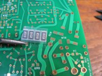
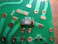
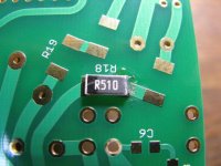
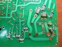
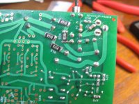
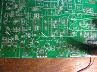
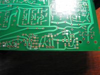
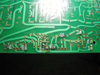
Power supply section, RCA input RF filter, output resistors
Here are some photos of the build-up of the power supply section, the resistors and capacitors around the rear RCA input, and the twelve 0.5R output stage resistors. I'm including those RCA input parts and output stage resistors just because they are in the vicinity, even though they don't have anything to do with the power supply.
Everything in the power supply section but the 4 regulator chips and the two large 560uF caps will be installed. I'm leaving those out just becuase it is easier working on the rest of the board without tall parts sticking up. Same for the rear (and front) RCA jacks - I'll leave those out until the very end since they are tall. And same for the 6 output chips and associated bypass caps. Those SIP packages are rather tall. Easier to get the soldering iron to parts in the gain stage without those in yet.
All the surface mount parts (all resistors) are on the bottom of the PC board again in this section. All the through-hole parts are on the top again. Best to complete the surface mount parts on the bottom of the PCB first again, then do the through-hole stuff on the top.
When soldering the surface mount parts try to be careful not to get solder on adjacent though-holes. If solder does get on a through-hole and plug it up you will need to use some desoldering wick or a desoldering suction bulb to get it out before the through-hole lead will fit through. Another trick is stick the lead in as far as it will go, heat the bottom of the lead near the hole, and let the hot part lead melt the solder plug in the hole.
I would also highly recommend ordering one additional part of each of the smaller 1206 sized SMD's if you can. It is just soooo easy for them to suddenly flip or slip off the tweezers or board onto a rug or who knows where, never to be seen again. For 50 cents or so for the SMD resistors it is a lot cheaper getting an extra than having to re-order from mouser for one or two lost parts. During my soldering of just this example I had two SMD parts and one through-hole part flip off and land on the rug. I found all three this time, but I'm usually not so lucky. Those are the odds you are up against!.
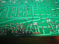
* The first two photos show the top and bottom of this section of the PC board.
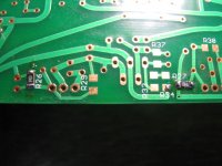
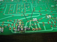
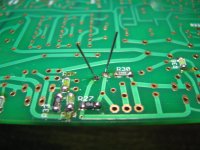
* There is no order the surface mount resistors have to be done in. I just randomly started at the left. Many of the parts in this section have the same value part used in two places (once in the positive regulator and again in the negative regulator). It is easiest to just to sodler in both resistors once you have that particular part bag from Mouser open. For example I started with R26 in the next photo, a 3.4K from the BOM, which is also used in R27. I just went ahead and soldered them both in, as in the photo. Then the next part along the way is R29, a 249R resistor that is also used in R30. Soldered both of those in, etc. Just work your way across like that.
* The next photo shows all 10 of the surface mount resistors in this section soldered on now. The revised build instructions will call these out by part number.
* On to the through-hole parts on the top of the PCB. Again no order anything has to be done in, but always a good idea to solder in interior parts first that might be blocked by things around it.
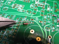
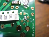
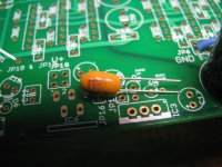
* The next two photos shows one of the four 10uF tantalum capactors (C17, 18, 20, 21). You can just barely see the little "+" symbol on the capacitor with a manifying glass, next to the vertical bar. That lines up with the "+" on the board, like in the C17 position in the photo. Very important that the tantalums are in the right way. They are not happy campers if in backward. Worth double-checking all the "+" sign orientations once they are in.
* The next three photos show what I posted in the CRC section write-up about bending the through-hole part leads at about a 30 degree angle to hold them while the board gets flipped upside down to solder. Then solder one lead and check the part orientation on the top side. Push down while heating the one lead if needed to drop the part down closer to the board. Then solder up the remaining lead and clip off the excess.
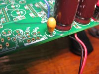
* The final photo shows how to orient the two 22uF 35V solid polymer caps (C35, 36). That dark half on the top is the negative lead side, while the PC board is marked on the positive side.
Here are some photos of the build-up of the power supply section, the resistors and capacitors around the rear RCA input, and the twelve 0.5R output stage resistors. I'm including those RCA input parts and output stage resistors just because they are in the vicinity, even though they don't have anything to do with the power supply.
Everything in the power supply section but the 4 regulator chips and the two large 560uF caps will be installed. I'm leaving those out just becuase it is easier working on the rest of the board without tall parts sticking up. Same for the rear (and front) RCA jacks - I'll leave those out until the very end since they are tall. And same for the 6 output chips and associated bypass caps. Those SIP packages are rather tall. Easier to get the soldering iron to parts in the gain stage without those in yet.
All the surface mount parts (all resistors) are on the bottom of the PC board again in this section. All the through-hole parts are on the top again. Best to complete the surface mount parts on the bottom of the PCB first again, then do the through-hole stuff on the top.
When soldering the surface mount parts try to be careful not to get solder on adjacent though-holes. If solder does get on a through-hole and plug it up you will need to use some desoldering wick or a desoldering suction bulb to get it out before the through-hole lead will fit through. Another trick is stick the lead in as far as it will go, heat the bottom of the lead near the hole, and let the hot part lead melt the solder plug in the hole.
I would also highly recommend ordering one additional part of each of the smaller 1206 sized SMD's if you can. It is just soooo easy for them to suddenly flip or slip off the tweezers or board onto a rug or who knows where, never to be seen again. For 50 cents or so for the SMD resistors it is a lot cheaper getting an extra than having to re-order from mouser for one or two lost parts. During my soldering of just this example I had two SMD parts and one through-hole part flip off and land on the rug. I found all three this time, but I'm usually not so lucky. Those are the odds you are up against!.
* The first two photos show the top and bottom of this section of the PC board.
* There is no order the surface mount resistors have to be done in. I just randomly started at the left. Many of the parts in this section have the same value part used in two places (once in the positive regulator and again in the negative regulator). It is easiest to just to sodler in both resistors once you have that particular part bag from Mouser open. For example I started with R26 in the next photo, a 3.4K from the BOM, which is also used in R27. I just went ahead and soldered them both in, as in the photo. Then the next part along the way is R29, a 249R resistor that is also used in R30. Soldered both of those in, etc. Just work your way across like that.
* The next photo shows all 10 of the surface mount resistors in this section soldered on now. The revised build instructions will call these out by part number.
* On to the through-hole parts on the top of the PCB. Again no order anything has to be done in, but always a good idea to solder in interior parts first that might be blocked by things around it.
* The next two photos shows one of the four 10uF tantalum capactors (C17, 18, 20, 21). You can just barely see the little "+" symbol on the capacitor with a manifying glass, next to the vertical bar. That lines up with the "+" on the board, like in the C17 position in the photo. Very important that the tantalums are in the right way. They are not happy campers if in backward. Worth double-checking all the "+" sign orientations once they are in.
* The next three photos show what I posted in the CRC section write-up about bending the through-hole part leads at about a 30 degree angle to hold them while the board gets flipped upside down to solder. Then solder one lead and check the part orientation on the top side. Push down while heating the one lead if needed to drop the part down closer to the board. Then solder up the remaining lead and clip off the excess.
* The final photo shows how to orient the two 22uF 35V solid polymer caps (C35, 36). That dark half on the top is the negative lead side, while the PC board is marked on the positive side.
Attachments
-
 IMG_2418.JPG57.1 KB · Views: 65
 -
 IMG_2417.JPG105.8 KB · Views: 59
 -
 IMG_2416.JPG69.4 KB · Views: 81
 -
 IMG_2421.JPG70.6 KB · Views: 59
 -
 IMG_2423.JPG64.9 KB · Views: 57
 -
 IMG_2426.JPG56.8 KB · Views: 63
 -
 IMG_2427.JPG64.4 KB · Views: 61
 -
 IMG_2428.JPG58.9 KB · Views: 57
 -
 IMG_2429.JPG60.1 KB · Views: 60
 -
 IMG_2431.JPG95.9 KB · Views: 74
Last edited:
- Home
- Amplifiers
- Headphone Systems
- A version of an O2 Desktop Amp (ODA)