I agree that adding unequal flip-flop delays is a good idea now that everything works with perfectly matched flip-flops.
Are the attachments usable? normaal.txt is Free Pascal source code with the extension changed from .pp to .txt to pass the forum software. delays.txt is the result of a run. The delays are in nanoseconds and are exaggerated to make the simulation less critical, like your earlier simulations, although I reduced the systematic difference between rising and falling delay to 10 ns.
The flip-flops are numbered as they appear in the shift register, not according to any schematic. Flip-flops 1 and 2 are supposed to be on the same chip, the same holds for flip-flops 3 and 4.
Everything is based on wild guesses and exaggeration, but that shouldn't matter when you just want to know what concept can handle flip-flop delay variations best.
By the way, I retrieved my filter calculations from the attic. I have to look if they are in a form that I can still understand after 5 years and scan them.
Attachments
Last edited:
Hans, regarding the calculation of C58, do you need the whole derivation or just the equations that came out of it?
What I retrieved from the attic is not in a state where I can fully understand it myself, as there appear to be parts missing. Basically what I've done is this:
A. For the calculation, replace U6A, R90, R101, R87, C51 with an LR parallel network: L = (R90 + R101)*C51*R87 and R = (R90 + R101) in parallel with R87. (By the way, R90 is a phase correction resistor that wouldn't be needed if the op-amp were ideal. R101 would then be 2.69 kohm, so the sum of the present R90 and R101.)
B. For the calculation, replace R92, R105, R108, R111 with one resistor equal to their parallel value.
C. Solve the network equations (I used modified nodal analysis) and write out the characteristic polynomial.
D. Calculate the polynomial coefficients corresponding to the desired poles. That is, multiply (-s/p1 + 1) (-s/p2 + 1) (-s/p3 + 1), where p1, p2 and p3 are the intended poles, to find what coefficients s^3, s^2 and s should have.
E. Find a way to choose some component values and calculate the others, such that you can find closed-form expressions for them. Apparently this was the most difficult part and I didn't quite succeed, one value was found iteratively. I ended up choosing C58, C59 and the parallel value of R92 // R105 // R108 // R111 // R100 and calculating the rest. I found closed-form expressions for the LR network of step A, but not for the ratio between R100 and R92 // R105 // R108 // R111.
I have the equations of step E, but some of the derivation appears to be lost.
Marcel,
Thx, your explanation regarding the 3.3nF is more than enough, I will find my way to further solving this.
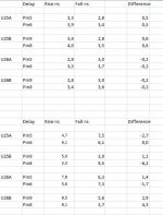
About the suggested FF delays, I think they are too conservative for this test, see upper part of the table below.
The 74AC74 has a typ. delay of 6nsec, with a min/max of resp. 2.5nsec and 10.5nsec.
That's why I made a Gaussian distributed random number series with an average of 6.0nsec and a SD of 2.0nsec.
See lower part of the table below with the generated 16 numbers.
For the SIM running at 2.5Mhz, I will multiply these figures by 10.
Hope to come back soon with the results.
Hans
.
Thx, your explanation regarding the 3.3nF is more than enough, I will find my way to further solving this.
About the suggested FF delays, I think they are too conservative for this test, see upper part of the table below.
The 74AC74 has a typ. delay of 6nsec, with a min/max of resp. 2.5nsec and 10.5nsec.
That's why I made a Gaussian distributed random number series with an average of 6.0nsec and a SD of 2.0nsec.
See lower part of the table below with the generated 16 numbers.
For the SIM running at 2.5Mhz, I will multiply these figures by 10.
Hope to come back soon with the results.
Hans
.
Attachments
I didn't realize you wanted realistic values, I thought exaggerated values were preferred so the simulation doesn't need to be too accurate.
If you want it to be realistic, the overall standard deviation is more likely to be 1 ns...1.3 ns than 2 ns. 2 ns would lead to serious yield loss with those specifications. Besides, there will always be a small systematic difference between the delays to the positive and negative outputs, because the logical path is usually 1 internal gate longer or shorter, and there will be less spread between flip-flops on the same chip than between flip-flops on different chips. See the attachments for a counter-proposal.
If you want it to be realistic, the overall standard deviation is more likely to be 1 ns...1.3 ns than 2 ns. 2 ns would lead to serious yield loss with those specifications. Besides, there will always be a small systematic difference between the delays to the positive and negative outputs, because the logical path is usually 1 internal gate longer or shorter, and there will be less spread between flip-flops on the same chip than between flip-flops on different chips. See the attachments for a counter-proposal.
Attachments
Yes, I used a bit exaggerated figures with the SD of 2.0, and yes, within the same chip difference are likely to be smaller, although not specified.
But here are the first results:
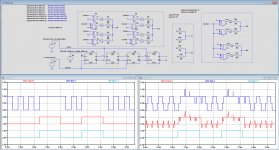
1)With the two versions that are mixed with the clock signal, FF delays do not play any role in the result, because the clock is completely masking this.
The version with resistors only, does not function properly with differing delays of the FFs. For that reason I concentrated first on the two Gated versions only.
2)However when applying delays on the gates, awkward signals are produced with the delays used because of all the spikes caused by the different output delays.
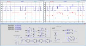
Delays can be switched between 0.1nsec for all delays, or to the other table in the upper left corner in the circuit diagram below.
Of course with 0.1nsec everything works perfectly as shown below left, while with delays switched on to the right it becomes a mess.
The gate delays are thus a very important factor and I must say, the result is worse as expected.
As a next step I will use the figures you just gave.
Hans
.
But here are the first results:
1)With the two versions that are mixed with the clock signal, FF delays do not play any role in the result, because the clock is completely masking this.
The version with resistors only, does not function properly with differing delays of the FFs. For that reason I concentrated first on the two Gated versions only.
2)However when applying delays on the gates, awkward signals are produced with the delays used because of all the spikes caused by the different output delays.
Delays can be switched between 0.1nsec for all delays, or to the other table in the upper left corner in the circuit diagram below.
Of course with 0.1nsec everything works perfectly as shown below left, while with delays switched on to the right it becomes a mess.
The gate delays are thus a very important factor and I must say, the result is worse as expected.
As a next step I will use the figures you just gave.
Hans
.
Attachments
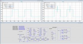
Now I used the latest figures you gave, see the table in the circuit diagram.
Things are better, but not perfect.
It seems like having to make a choice between the gate delays where the delay of the FFs is not playing any role bit with lots of glitches, or alternatively for the version without gates that uses resistors directly connected to the FFs and take the FF delays for granted.
Both results are visible below.
For the resistor only version, giving 6dB more output, just 0.3% difference in average value between without and with added delay doesn't seem that bad.
But before jumping to conclusions, I will again make a table with average values for all three versions, with the 0010100 and the 0011000 pattern,
With and without differences in delay.
Hans
.
Attachments
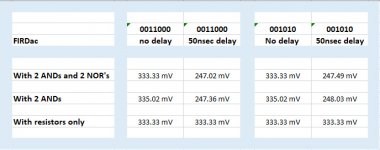
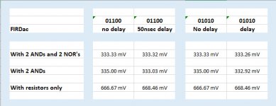
Here are all the figures for the 3 versions.
Simulation was done with a 2.5Mhz signal, with 0.1nsec resolution.
On top is the resistor only version with no difference between 01010 and 01100 with the delay given in #68.
Second the 4 gate version and
Last the 2 gate version.
Hans
.
Simulation was done with a 2.5Mhz signal, with 0.1nsec resolution.
On top is the resistor only version with no difference between 01010 and 01100 with the delay given in #68.
Second the 4 gate version and
Last the 2 gate version.
Hans
.
Attachments
As mentioned, with the two versions using gates, delay of the FFs plays no role at all as long as the FF delay< 1/4 clock and for that reason the FFs where not delayed, so the delays could be used for the gates.
On the other hand when measuring the resistor only version no gates are used and the delays are now used for the FF's, because with resistors only the delay of the FF's is vital to include.
Hans
On the other hand when measuring the resistor only version no gates are used and the delays are now used for the FF's, because with resistors only the delay of the FF's is vital to include.
Hans
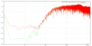
These are simulation plots of the DFT of the output signal of my PWM8 modulator with and without pattern-dependent bit weights, the input signal is a small DC offset. Green is the ideal case, red is when the weight of a 1 becomes 0.1 % larger when the preceding bit was also a 1. The spectrum flattens below 50 kHz with the 0.1 % error. The results look much more scary when you use a modulator with big idle tone around fs/2, like plain single-bit modulators.
The vertical axis is in dB with respect to an arbitrary reference, the horizontal axis is in kHz. It's a DFT with Hann window and 1 kHz bin size and the modulator runs at a slightly higher clock frequency than in reality, 28.224 MHz instead of 27 MHz.
The vertical axis is in dB with respect to an arbitrary reference, the horizontal axis is in kHz. It's a DFT with Hann window and 1 kHz bin size and the modulator runs at a slightly higher clock frequency than in reality, 28.224 MHz instead of 27 MHz.
Attachments
After thoroughly checking, a small typo was found in the sim resulting in a faulty table in posting#72.
Here is the corrected table, where also the effect of a 45% a duty cycle is added.
Clock is 2.5Mhz, and with 0.1nsec resolution the average value is measured by LTSpice for the patterns 01100 and 01010.
Delays used are as proposed in Marcel's posting #68.
The Resistor Only version is completely insensitive to clock duty cycle, and is also the most stable version with the used delay table plus giving a bonus of 6dB extra output.
Hans
.
Attachments
I now used a much more aggressive table and redid the Resistor Only version.
Despite the large differences in rise and fall time with this table, this version responded without any drama and stayed as stable as before.
For the 01010 and the 01100 patterns without delay is twice time the same previous 666.67 mV.
Now with the aggressive delay, that's more severe than worst case, the average values for both patterns gave now again twice exactly the same value with 669.17 mV, stable as a rock.
See table below for the two delay patterns used, above a realistic version from Marcel and below the aggressive version used for this test.
From the tests performed so far, the Resistor Only version seems the most resistive to rise and fall time differences and variations in clock duty cycle.
Hans
P.S. Because I used a clock 10 times slower, all delays in the table were multiplied by 10.
.
Attachments
Last edited:
- Home
- Source & Line
- Digital Line Level
- 74AHC02 and 74AHC08 DAC with 97 dB(A) dynamic range