Info from TI Topic 6
This is a gate drv I have used in the past:
Wound on toroid 846T250-3C8
Al = 1650 mH/1000T
Primary = 12 T Lp = (12/1000)**2 x 1650mH = 230uH
If the IC supply is 15 V then in your case you would have
15V * 3uS/230uH = 100ma of primary current
then 12 x 230uH X (100mA)**2 = 1.2uJ
and this core can store 16uJ .
I don't think the gatedrv is the problem, unless the deadtime is too small. The problem I think is the sizing of the inductor. I think the inductor was sized to support an idle current. They are coupled and your supply sees 900uH . If you caculate 1/4 x Iload then the inductor value will be close to 200uH and that would be 100uH in each leg of output. Large inductors will be hard to compensate in current mode with most controllers that don't support skip-cycle. Since you have Chris Basso's book this is covered in all current mode simulations.
The slope of the inductor should closely match the slope of the osc ramp. The slope of the inductor can be scoped across the ESR of the output cap or you can add a .1 ohm resistor in series with output cap for test. Should work.
chas1
I'd say it's either the inductor or the gatedrive ")
I've put together a very useful circuit that lets me test inductors, I believe there was a similar one posted by Eva long ago too. It lets me test the inductance and saturation currents of various SMPS components. It's essentialy a boost converter with a current sense resistor connected to the oscilloscope. The slope of the ramp wave can be read on the oscilloscope to calculate inductance and it will show the kink when saturating.
In his converter he could just probe the current sense resistor to see if the output inductor is saturating.
The reason I suspect gatedrive is because single ended converters with gate drive transformers is a pretty seldom covered topic and it's easily overlooked that DC blocking and DC restoration or other means of drive transformer reset is needed. Else the gatedrive transformer will saturate due to the DC bias. And that leads to collapse of the power supply to the switching chip.
proper phasing of inductors
mag
How are the windings of the inductor laid on the core, I am sure you checked this but the should be phased correctly ,the postive and negative supply should be connected to opposing ends.
Some info from the Ridely website:
PWM chip Output Drivers do not like to see inductive loads. If you are driving a gate drive transformer you may see a problem in the drive signal, manifesting itself as a double output pulse with a brief dropout period.
If you don't see this problem in the lab, don't assume it won't be there in production. The magnetizing inductance of the gate drive transformer can vary substantially over time, core lot, temperature, etc. Make sure you consider the worst case scenario before deciding you don't have this problem.
Unitrode recommends the use of catch diodes to eliminate the problem.
Another alternative is to parallel the transformer with a resistor.
chas1
info
you might find useful info here:
www.powersystemsdesign.com/design_tips_dec06.pdf
A appnote from Ridely's website on gate drive transformer connection.
chas1
you might find useful info here:
www.powersystemsdesign.com/design_tips_dec06.pdf
A appnote from Ridely's website on gate drive transformer connection.
chas1
single ended
mega
No, I only work with FB & HB at present but in the past I connected the cntrl IC output thru suitable resistor/diode to lower mosfet and the upper thru res/cap in series with primary of gatedrv tranny .1uF & 4.7 ohms seem to work well but the new IC's need a buffer most of time therefore a npn/pnp combo driving the primary thru .1uF with a 1n914 bypass and returned to top of sense resistor should do the trick in a forward converter.
If needed I would be happy to provide schematic of both along with sims in LTspice.
chas1
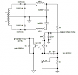
Hi chas1 and megajocke,
attached you will find a schematic of the gate drive transformer circuit.
As I have stated before there is no substantial difference between this and the circuit with ir2110. in the current prototype I have put back in place the IR2110.
I have ordered some ncp1216a from onsemi and I am waiting for the delivery.
Attachments
explanation of testing
mag
I think you mentioned that you have simulated your supply if so what sim software did you use. Did you only simulate the postive with the output circuits shown in the schematic and a load . The gatedrv circuit is ok and shouldn't be a problem.
chas1
mag
I think you mentioned that you have simulated your supply if so what sim software did you use. Did you only simulate the postive with the output circuits shown in the schematic and a load . The gatedrv circuit is ok and shouldn't be a problem.
chas1
I agree, the gate drive looks like it isn't what is causing the problem. Though it has a problem - for the first cycle the gate is driven with ~30V.
Is what happens that the circuit latches off and the supply needs to be cycled for it to restart? The control IC has a latching protection that is reset by the UVLO. This must be activating, so it's either overcurrent being detected (layout problem, leading-edge spike or saturation), overvoltage on the driver supply or the OLP being triggered.
I'd suspect the OCL in first hand, either saturation of the output inductor or increased leading edge spike because of output rectifier reverse recovery. It could also be the increased noise from reverse recovery disturbing the control circuit.
mag said:Hi all,
I have stabilized the feedback loop but now I still have some probelems with the current mode control.
As soon as I increase the load the smps start to continously turn on and off.
I have measured the voltage on the Isns pin of FAN7554 and I see very high peaks even with 10mA load.
I have captured with the scope the waveform across the current limit resistor (in attached). Those spikes are huge (from +30V to -20V with no load). I suspect that I have too much inductance on the current sense resistor (0.22ohm, 3W, wirewound!!).
Should I replace the resistor with something not wirewound?
Slowing down the mosfet gate charge time (increasing the gate resistor) can be effective?
thank you
I made allmost the same power supply using an L6385 (with an external diode to charge the bootstrap capacitor) and an UC3845.
>>
As soon as I increase the load the smps start to continously turn on and off.
>>
You get this type of behaviour if the transformer windings are reversed.
(Magetizing current will tell you what is going on.)
And, I also see that you are having problems charging the bootstrap capacitor of the gate driver. This should not be a problem. The upper side of the primary winding is connected to ground trough D7 during the off-time. During startup the lower MOSFET will connect HS_S with ground and Q2 will close a little later. But that shouldn't be a problem. D19 and D20 are not required. Just place 4.7Ohm resistors in series with D15 and D16. (Sort of peak detectors) This way you still have 12V while you can limit the output power of the highvoltage outputs. (The peak voltage on the windings are allways the same)
My power supply is working very well, and current limiting is excellent in a way a half bridge can't. No flux walking whatsoever. No mosfet's got killed. Only two L6385 drivers because the don't like more then 18V. A 15V zener curred the problem.
By the way, you can size the inductors on the high voltage rails to get short circuit proof current limiting. Just stare a few seconds at DI in the output inductors.
Regards
I forgot, you need current sensing resistors with a very low self inductance.
Something like Welwyn WP-S series comes very close.
welwyn-tt.com/pdf/datasheet/WP-S.PDF
If you don't know what you have, just brake on into pieces with a hammer count the windings and calculate the self inductance. Then you know how large a spike you can expect if you know what current and how fast you are switching.
Routing of the current limit signal is very important. Star grounding and other techniques can help.
My version1 PCB has past the conducted emission test with minor modifications.
Hendrik
Transformer
mag & mega
What about transformer, How are the windings laid on and do you have shields included in the transformer . mine are wound in this form /shield / 1/2 primary / shield / secondary / shield / remaining primary and a aux winding if required. I am currently simulating the circuit in LTspice as was described (only using the postive supply) and then I will add negative terminated only with the output caps and no load and see if that not the problem. I don't use orcad and thats why I ask for your sim schematic so I can compare results.
chas1
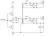
Hi Chas1,
attached you will find my simulation schematics; as you can see there is no negative rail at all. Also on my prototype I have disconnected the output diode for the negative rail from the transformer.
My transformer is wound in this way:
1) Primary1 (3 wires in parallel)
--shield--
2) Secondary1 (6 wires wound in bifilar)
--shield--
3) Primary2 (3 wires in parallel) + Auxiliary winding
--shield--
4) Secondary2 (6 wires wound in bilifar) + Low voltage secondary (bifilar)
After that primary1 is in parallel with primary1 and secondary1 is in parallel with secondary2.
The measured primary inductance is Lmag=1.4mH, this will apply a slope compensation of Se=Vin/Lmag*Rsense=14.7kV/s.
@hendrik
Thank you very much for your suggestion about the transformer winding direction. It was not my intention of course but it worth to check if the direction is right.
Current sense resistor: I have put in parallel two resistors of 0.22R 3W, I have then measured the inductance of that combo with a network analyzer and I got 25nH. Then I have placed a low pass filter to compensate the zero created by the parasitic inductance of the sense resistor (fzero=Rsense/(2*pi*Lsense)=700kHz). A low pass filter with R=2.2k and C=100pF can do the job.
Can you please clarify the point about the 12V generation? If I remove the diodes D15 and D16 I should also remove the inductances L2 and L3. In this way it becomes a peak rectifier and the winding on the transformer must be changed. What is the advantage of doing this? My TL431 + opto are powered from the +12V output, can a problem on the 12V output jeopardize the feedback stability?
thank you
Attachments
- Status
- This old topic is closed. If you want to reopen this topic, contact a moderator using the "Report Post" button.
- Home
- Amplifiers
- Power Supplies
- 500W offline SMPS