Very good!
Schurter 3101.0045 looks more stable and is up to 16A:
http://www.mouser.at/ProductDetail/Schurter/31010045/?qs=%2fha2pyFaduiCLpZ5DeJEqJGs0HKZmj9jCrT76cTDpNI%3d
I could add a universal footprint. So you can use many different fuse holders.
Would this be OK for you?
BR, Toni
Probably a better product. Don't make changes for me unless it shrinks the board. I have spare Schurter horizontal mount fuse holders which are much cheaper. I just took a look at vertical mount parts because of the space efficiency. The Bulgin caught my eye only because there is an existing footprint in KiCad for it.
")
I think I made a mistake when I calculated this before. I think the number should be more like 7.5W per 4-diode bridge. At least that is what I see now and I can't see that I have made any significant changes.
It depends on the used diode model and the temperature too...
6 - 8 W is the maximum power dissipation here when using Schottky diodes. But who listens to 400W@4R continuous sinus output power?
Audio crest factor is 10 - 15% hence diode power dissipation very low.
Of course we love to design an amplifier that is able to deliver continuous output power ...
BR, Toni
Last edited:
Think both products are OK. The vertical fuses could be a good option for the smaller power supply board (for e.g.: SA2015/16) with only 4 big lytics to save space...Probably a better product. Don't make changes for me unless it shrinks the board. ...
BR, Toni
Yes, of course, but I made no changes to the model there. I'm not sure why I got 5.7W before. Probably just stupid error.
And indeed designing for 400W@4R is exceedingly aggressive - and why there's likely good space economy to be had from "optimising" diode heat sinking in the supply.
And indeed designing for 400W@4R is exceedingly aggressive - and why there's likely good space economy to be had from "optimising" diode heat sinking in the supply.
It's all in having good libraries to start with. If you noticed, it is a placed layout with no routing yet. Although there are not that many nets, based on the guides that I see . For a design like this it should be a bunch of area fills, so routing should be fairly easy to do.I don't know how you work so fast
What layout package is Tony using?
Oh I am just curious what he uses, I use Orcad 16 and make by own footprint/libraries, it is very time consuming. Practice makes perfect, esp if you add all the graphics to make it look like real life in the case of a HS, with all the extrusion cuts to maximize the surface area. Then it becomes more art than function.
It is a shame that it is near impossible to trade footprints between eCAD tools.
It is a shame that it is near impossible to trade footprints between eCAD tools.
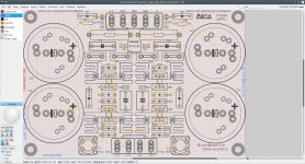
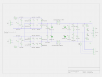
SA2015/SA2016 power supply ...
150x90mm ...
BTW: have tested clip mount using SK481, MBR40250 and a THFU1. Very hard to insert the clip, even harder to remove it. For the SK489 variant we would need 8 clips ...
For maintenance it is better to use the screw mount based SK75/SK76 ...
BR, Toni
150x90mm ...
BTW: have tested clip mount using SK481, MBR40250 and a THFU1. Very hard to insert the clip, even harder to remove it. For the SK489 variant we would need 8 clips ...
For maintenance it is better to use the screw mount based SK75/SK76 ...
BR, Toni
Attachments
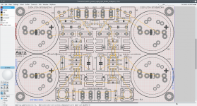
SA2014/SA2015/SA2016 power supply ...
ready for fab ...
Note: Schematics are free to use only for non commercial DIY projects.
WARNING: the circuit is using and providing very high AC and DC voltages and is therefore very dangerous and can be lethal. I am not responsible for any costs, damage and/or injury using these schematics. Do not use this schematics if you do not have the necessary experience and knowledge.
This power supply can be used for SA2014 and with an alternative schematic and BOM also for SA2015 and SA2016 amplifiers.
BR, Toni
Attachments
Last edited:
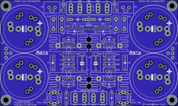
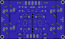
Hi. I have a question regarding your ground plane structure. On the bottom of the board you have thermals from the main filter caps to isolated ground planes on the bottom of the board. Don't we ideally want the pulses from the caps of both rails to circulate, and cancel, amongst each other? Hence it would be better to encourage those pulses to circulate immediately on your top layer ground plane rather than down to a relatively isolated plane connected only by the cap pins and 4 vias each. I would delete the isolated planes on the bottom of the board (and the vias).
Nice job providing for both fuse packages.
Lastly, why do you plate the mounting holes?
(I keep tinkering with a version (3 large caps per rail) in KiCad. It may never go to production, but it is better to attempt to learn the pcb software with a specific project which might just be useful rather than laboriously reading a manual. )
Nice job providing for both fuse packages.
Lastly, why do you plate the mounting holes?
(I keep tinkering with a version (3 large caps per rail) in KiCad. It may never go to production, but it is better to attempt to learn the pcb software with a specific project which might just be useful rather than laboriously reading a manual.
)I repeatedly state that the two wire intermodule connection use close coupled wire pair.Don't we ideally want the pulses from the caps of both rails to circulate,
Why would you want currents to circulate?
Intermodule connection? I'm talking about current flows on the PSU board. The close-coupled wire pair which leaves this board is Vcc and Vee. You want the ground wire well clear of them.
"circulate locally, and cancel, amongst each other" - I omitted "locally". Why allow a path across the bottom of the board and up a via when the ground plane is on the top layer?
It also suggests the - pins of the +ve rail filter caps be as close as possible to the + pins of the -ve rail (rather than the opposite). No?
Last edited:
I am very interested in building this. Are parts and PCBs in the Netherlands? If so, at what cost? Where can I find the current schematics, sorry that I haven't read through the entire. Just found this 15 minutes ago. Also, are there photos of finished builts of this project?
transformer to rectifier, rectifier to smoothing capacitor, smoothing capacitor to second stage. etcIntermodule connection?
NO !I'm talking about current flows on the PSU board. The close-coupled wire pair which leaves this board is Vcc and Vee.
Vcc and power Zero Volts is one circuit. Vee and Power Zero Volts is a second circuit.
Vcc must be close coupled to Zero Volts. Vee must be close coupled to Zero Volts.You want the ground wire well clear of them.
The intermodule connection from PSU to load is the twisted triplet of Vcc+Vee+Zero Volts.
You have to understand the route that the current NEEDs to make. Then see where the PCB allows that route to be. Then after you have made that analysis are you ready to offer advice on how he should arrange his traces."circulate locally, and cancel, amongst each other" - I omitted "locally". Why allow a path across the bottom of the board and up a via when the ground plane is on the top layer? .............
I have not analysed his PCB traces nor the routes that the current needs to flow so I'm not going to offer that advice.
- Home
- Amplifiers
- Solid State
- 2stageEF high performance class AB power amp / 200W8R / 400W4R