Can you see the difference.
Not everything tad the sell in baan moo really works, sometime,s the sell fault Pcp,s.
Modify it after my Plan and it will Work.
")

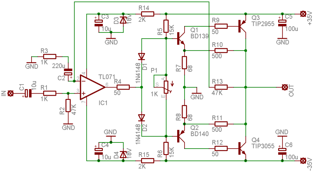
Hi folks, one question that I have about the circuit is if the output impedance is low enough to drive speakers in the range of 4 ohms because the power transistors operates as common emitters versus the typical common collector configuration on most power amp designs.
Would this configuration on power performance at very low impedances acceptable?
In most audio discussions here, the design of this output stage is simply called a CFP - aka Complementary Feedback Pair or Szlikai Pair. In use, the CFP output stage has marginally higher power output and efficiency than more common EF (Emitter Follower) designs. The popular P3A design is also a CFP.
I think you are mistaken in thinking there is there will be less current output than an equivalent EF design can deliver but the ability to use a triple EF arrangement for higher current gain is not there, if that is necessary for lower than 4Ω loads. With only a single pair of low gain 3055/2955 transistors, you may need more current gain from the stage than either simple type can provide with these.
However, this overall design has voltage gain in the output stage as part of the unique capability of CFP designs. Otherwise, because the voltage amplification of the TL071 is limited by its +/-17V max. supply rating, it could not drive the output stage to it's limits and an EF output stage would deliver only around 16W/8R. With perhaps +/- 22V power rails, you could have an appropriate match but much less power output than you might have imagined. Still, it would then have no problem driving even 2Ω loads.
Last edited:
Thanks for the explanation about the Szlikai Pair output stage (mentioned previously). The idea is to build an easy amp using a 2.54mm PCB matrix board. I have a 29 + 29 150W AC transformer and heatsinks (scratch from an older Sony HCD-DX2) which gives approx 40 + 40 volts rectified. The integrated Sony STK402-090S amp supposedly works fine but from my point of view and high number of burned devices STKs are not strong for high power endurance (STKs are very easy to destroy).
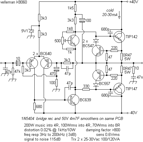
By the way an interesting circuit using only discrete components is the Velleman K8060.
I will see what to build despite the lack of overheating, short circuit and overload protections. Reusing an older 19 inch rack DJ amp case with two built-in fans (continuous cooling) thermal overheating on the power transistors is avoided.
The idea is to build an easy amp using a 2.54mm PCB matrix board. I have a 29 + 29 150W AC transformer and heatsinks (scratch from an older Sony HCD-DX2) which gives approx 40 + 40 volts rectified.
A single pair of 3055/2955 won't do on +/-40V. If they are selected for voltage (most will do 100V but you need to test them) you still need a pair in parallel. If you're wanting a single low cost pair for +/-40V, use TIP35C/36C.
Q1,2 need collector resistors, and Q3,4 need emitter resistors. Then you can parallel outputs. PLX3402 is this circuit on steroids. First stage is cascode, 2nd stage darlington with parallel outputs. It will take work to get stable when 'enhanced', but obviously not impossible.
well things may be not impossible in theory, but whether its a good idea or not is highly debatable for 90% of readers on this page. this circuit is a twitch fest , how to bias and test the 'standard one' would better for all involved, lets not add more uncertainty on the bench.
Last edited:
I've never been convinced that the CFP with gain performs as well as either the standard CFP or EF output stage. You could use a level shifter to drive the output stage as a normal EF (or CFP) stage. Basically you would use the driver transistors as you have but mirror them at the +/- Vcc rails, and as they then operate over the full voltage you can drive your output stage as normal.
John
John
CFP with gain in general doesn't perform as well as a unity gain OPS, and has more problems with cross conduction, reverse breakdown of the BE junctions, bias instability, and loop instability. The higher you push VCC the worse all this gets. It takes a well-refined circuit to beat the odds.
If you take the whole circuit and treat it as a low level front end and add a normal EF2 (EF3, etc) to it the situation is a lot better. Replace Q1,2 with small signal devices, and Q3,4 with VAS transistors. Add Baker clamps and Miller compensation to it. Then hook a Vbe multiplier between the collectors, add your unity gain output stage and dial in the amount of lead compensation required. It will need *some*- I've never got it to work with *none*. You can make a very high performing amplifier this way and the topology is scaleable to just about any size amplifier you want from 15 watts to 1500.
If you take the whole circuit and treat it as a low level front end and add a normal EF2 (EF3, etc) to it the situation is a lot better. Replace Q1,2 with small signal devices, and Q3,4 with VAS transistors. Add Baker clamps and Miller compensation to it. Then hook a Vbe multiplier between the collectors, add your unity gain output stage and dial in the amount of lead compensation required. It will need *some*- I've never got it to work with *none*. You can make a very high performing amplifier this way and the topology is scaleable to just about any size amplifier you want from 15 watts to 1500.
- Status
- This old topic is closed. If you want to reopen this topic, contact a moderator using the "Report Post" button.
- Home
- Amplifiers
- Solid State
- 2n3055 + mj2955 ampli