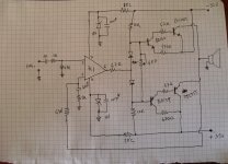
What should the bias current be ? The output device ares not included in the bias scheme, but they should not operate class B either or the loop is discontinuous.
they are, current at collectors of the drivers are fed to the bases of the output trannies......
The Vbe or base current of the outputs is not part of the bias control loop but it is controlled by it. The bias current from the driver essentially also flows into the base of the output devices.they are, current at collectors of the drivers are fed to the bases of the output trannies......
look at the small control loop formed by 2 diodes which controls both Vbe's of the drivers and the resulting bias current flowing thru the emitter resistors. The potentiometer controls by diverting the current from the diodes voltage. As someone else pointed out these two diodes should be thermally connected to the drivers for temp stability.
Last edited:
This circuit is sikmilar in some ways to the 'Texan' from PW in 1972. Interstingly, I have been playing with the idea of designing a small integrated 'fun' amp with similar features.
Advice above is good. However, make sure that initially you set VR1 for 0 ohms as measured between the bases of the two driver transistors. This will ensure that they are OFF. Then, as mentioned above, very slowly turn the pot up. You need to measure the collector current of one of the output devices - around 100mA is ok for a design like this.
You may have oscillation problems - do you have a scope?
first tests, I changed the two 1N4148 with 1N4007 I put two capacitors of 680pF between B and C of Bd139/140 I put two resistors 5W 220hom after the main supply
I changed the two 15k resistors in 10k.
then to +/- supply I plugged the tester (the only tool at my disposal)
I connected the black wire of the tester to the mass supply and the red to positive wire
I run the following measures:
after resistance of 220hom +21v and -29v
MJ2955
C = +17v
E = +21v
B = +21V
2N3055
C = +17v
E = -29v
B = -29v
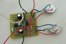
the wires that go from the PCB to the two manifolds are removed.
I have not connected the speaker and the input is open
could be reversed the two transistors BD139 and BD140?
I changed the two 15k resistors in 10k.
then to +/- supply I plugged the tester (the only tool at my disposal)
I connected the black wire of the tester to the mass supply and the red to positive wire
I run the following measures:
after resistance of 220hom +21v and -29v
MJ2955
C = +17v
E = +21v
B = +21V
2N3055
C = +17v
E = -29v
B = -29v
the wires that go from the PCB to the two manifolds are removed.
I have not connected the speaker and the input is open
could be reversed the two transistors BD139 and BD140?
Yes, I suspect oscillation.
A small cap across thhe feedback resistor is recommended.
just done whit 680pF
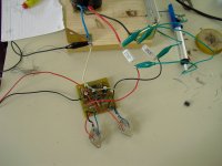
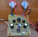
new test, I disconnected the power transistors as shown in the picture.
without speaker and open input.
I measured the voltage on the collectors about 20v
the transistor MJ2955 remains cold but the 2N3055 is very hot
all in about 10 seconds then turn off for fear that I end up burning everything.
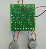
the history of the PCB:
I bought the pcb in my last vacation in bangkok
is virtually identical to the schema that I posted
The only difference is; I have two more capacitors in the power supply line
and the two resistors of 68hom that I removed
without speaker and open input.
I measured the voltage on the collectors about 20v
the transistor MJ2955 remains cold but the 2N3055 is very hot
all in about 10 seconds then turn off for fear that I end up burning everything.
the history of the PCB:
I bought the pcb in my last vacation in bangkok
is virtually identical to the schema that I posted
The only difference is; I have two more capacitors in the power supply line
and the two resistors of 68hom that I removed
Attachments
Last edited:
Oscillations can come from various sickness, asking for different medicine.Yes, I suspect oscillation.
A small cap across the feedback resistor is recommended.
About this toplogy that is using an op amp, a cfp current booster and global feedback.
I am aware of 3 caps:
The small cap across the feedback resistance is to limit the bandwith of the amplifier, usually at some 30Khz.
The cap at the output of the op amp to ground, is to prevent oscillations in the case the op amp is too fast relative to the booster. Usually, some 10nf to 100nf cap.
A small cap at a driver in the booster can remove oscillation.
See Rod Elliot explanations for details from Elliott Sound Products - The Audio Pages (Main Index)
Dad is the same AMP dad I buy,d in Thailand, and it Works Grate with an analog Power Supply, but it Oscillate,s with Switching-power
View attachment 219355
View attachment 219355
Last edited:
Dad is the same AMP dad I buy,d in Thailand, and it Works Grate with an analog Power Supply, but it Oscillate,s with a Switching-power wan.
View attachment 219350
I bought the PCB in "baan moo" the electronics district for 30 baht
anyway, does not work even after all the changes ....
Dad is the same AMP dad I buy,d in Thailand, and it Works Grate with an analog Power Supply, but it Oscillate,s with a Switching-power wan.
View attachment 219355
is not the same pcb
is not the same project
Attachments
Last edited:


What have I done wrong in my life??
I donut now?
Tray to lock at the Plan.

- Status
- This old topic is closed. If you want to reopen this topic, contact a moderator using the "Report Post" button.
- Home
- Amplifiers
- Solid State
- 2n3055 + mj2955 ampli