The low frequency roll-off is due to the power rail RC decouple to the IPS and the 1k load in the IPS cascode.
At low frequency they act as a divider for the Tian probe injection.
Need to think about what that means for loop gain but it seems my differential Tian probe implementation works fine.
Now I can accurately test whatever Damir, Richard Lee (or anyone else) comes up with.
Next step is a full Middlebrook2006 probe on the differential fixture and see if it makes any difference.
Best wishes
David
Hi David,
Could you confirm that this amp is stable?
Does Tian probe as I used it is good enough for stability analysis, or it needs to check internal loops too?
Thanks for your time
BR Damir
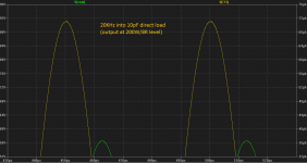
I was simulating 20kHz sine into direct capacitive loads before the output inductor with the Vertical MOSFET version and happened to notice something unusual (to me). The simulated current waveform has a kink or wrinkle on it even at 10pF load. At very large capacitance that wrinkle appears to be part of burst of oscillation. The voltage waveform, however, were all smooth in all cases and displayed no signs of instability.
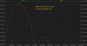
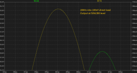
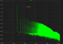
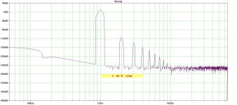
In cases of large capacitance, the FTT of Vout shows a slight elevation at about 3MHz, perhaps hinting the oscillation.
Is this a real indication of some sort of instability or is it a software artifacts? As the current wave form kink in the 10pF case is hard to understand. I did not do the simulation on the lateral MOSFET version so far.
Attachments
I was simulating 20kHz sine into direct capacitive loads before the output inductor with the Vertical MOSFET version and happened to notice something unusual (to me). The simulated current waveform has a kink or wrinkle on it even at 10pF load. At very large capacitance that wrinkle appears to be part of burst of oscillation. The voltage waveform, however, were all smooth in all cases and displayed no signs of instability.
In cases of large capacitance, the FTT of Vout shows a slight elevation at about 3MHz, perhaps hinting the oscillation.
Is this a real indication of some sort of instability or is it a software artifacts? As the current wave form kink in the 10pF case is hard to understand. I did not do the simulation on the lateral MOSFET version so far.
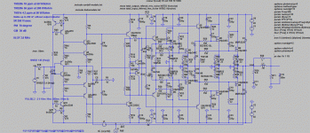
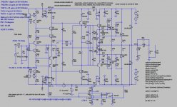
If you followed LMOS CFA then you could notice that I droped out RC parallel to feddback resistor(I think that you talk about C13 used there). It can inprove PM but not much and can lead to instability in CFA.
I suggest this schematic for VMOS and I attached zip file.
R1 is part of TPC but you don't need to use it, simulate and deside. It improve THD20k but not a lot.
BR Damir
Attachments
...Could you confirm that this amp is stable?
Does Tian probe as I used it is good enough for stability analysis, or it needs to check internal loops too?
The simulation looks quite stable to me. PM > 80 and GM> 20dB.
I haven't yet looked carefully at a comparison between the two methods but the
Tian probe in the outer loop does not seem sufficient for stability analysis.
Send me a PM with your Email address and I will send you my differential probe.
Best wishes
David.
If you followed LMOS CFA then you could notice that I droped out RC parallel to feddback resistor(I think that you talk about C13 used there). It can inprove PM but not much and can lead to instability in CFA.
I suggest this schematic for VMOS and I attached zip file.
R1 is part of TPC but you don't need to use it, simulate and deside. It improve THD20k but not a lot.
BR Damir
Hi Dadod,
C13 is a new cap I put across the Vout node and Ground as a direct capacitive load. My schematic was a capture from your #444 post, identical to the one in post #483in compensation topology and compensation component values.
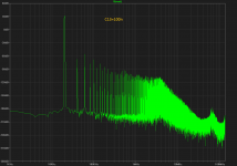
Your schematic in #483 displays the similar behavior as well. I stuck a 100n (happened to be C13 again) to the Vout and the wrinkle in capacitor current showed. See attached picture. It can also be verified by looking at the FFT plot for the floor elevation at about 3MHz. The elevation goes away if you set C13 = 1pF
I've just figured out the wrinkle in current waveform is part of the behavior near cross-over region of the output MOSFETs. Such transient related behavior probably will not show up in a small signal AC analysis.
I bias the OPS heavily at 200mA and the wrinkle improved, but I cannot say it was removed. Hopefully it is a benign behavior. But 800mA bias on +/-65V rails means a very HOT amp.
Attachments
...Does Tian probe... or it needs to check internal loops too?
For a Cherry amplifier with no internal loop then the outer loop probe is all you need.
Once you add an internal Miller loop then the outer loop becomes a less reliable indicator.
It looks like for this amp the outer loop is not an accurate predictor of stability.
This makes sense once you think about it - if the internal loop makes a substantial contribution to stability then it will also have a substantial effect on the loop gains and how they are distributed across the different loops.
So it seems if you stabilise with inner loops then you need to check the total return ratio and the outer loop is not reliable.
This is theoretically also true for ordinary Miller compensation but the typical VAS is sufficiently stable that it is not usually a problem in practice.
Best wishes
David
Hi Dadod,
C13 is a new cap I put across the Vout node and Ground as a direct capacitive load. My schematic was a capture from your #444 post, identical to the one in post #483in compensation topology and compensation component values.
Your schematic in #483 displays the similar behavior as well. I stuck a 100n (happened to be C13 again) to the Vout and the wrinkle in capacitor current showed. See attached picture. It can also be verified by looking at the FFT plot for the floor elevation at about 3MHz. The elevation goes away if you set C13 = 1pF
I've just figured out the wrinkle in current waveform is part of the behavior near cross-over region of the output MOSFETs. Such transient related behavior probably will not show up in a small signal AC analysis.
I bias the OPS heavily at 200mA and the wrinkle improved, but I cannot say it was removed. Hopefully it is a benign behavior. But 800mA bias on +/-65V rails means a very HOT amp.
I am not sure what provokes that, but I don't think it is instability. Do you want to drive capacitive load with no output inductor?
BR Damir
For a Cherry amplifier with no internal loop then the outer loop probe is all you need.
Once you add an internal Miller loop then the outer loop becomes a less reliable indicator.
It looks like for this amp the outer loop is not an accurate predictor of stability.
This makes sense once you think about it - if the internal loop makes a substantial contribution to stability then it will also have a substantial effect on the loop gains and how they are distributed across the different loops.
So it seems if you stabilise with inner loops then you need to check the total return ratio and the outer loop is not reliable.
This is theoretically also true for ordinary Miller compensation but the typical VAS is sufficiently stable that it is not usually a problem in practice.
Best wishes
David
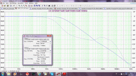
Inner loop gain thanks to David.
BR Damir
Attachments
...Please may I also have a copy of your ZTP for Damir's amp.
Sent, but I carelessly left an obsolete "subject" description, so don't put it in spam.
Best wishes
David.
of 'pure Cherry' over 2 pole Cherry is that it allows substantial PSR improvement by the addition of 1 ceramic cap. This is C1 in #4 of the tpc-vs-tmc-vs-pure-cherry thread.
The important caveat with this trick is that you need to make the strays symmetrical too.I liked that neat trick. Probably possible to extend the idea with an extra RC to add a pole/zero to C1.
The layout is critical and the 2 paths, one via the 'pure Cherry' cap and the other into the other side of the current mirror must be identical.
You have exactly the same problem doing balanced electronic i/ps on mixers. If you do really nice symmetrical PCB layouts, you get zillion dB CMR over a very wide frequency range without trims & other stuff.
My small brain has problems doing nice symmetrical layouts even for the simple 'pure Cherry' cap plus A N other. Having to route 2 caps + resistor on each path is too hard for me
")
BTW, this works with plain Miller too but THD levels with Miller are not usually small enough to see THD improvement though PSR is better.
PS I really want to join in the discussion on the CFA thread but need to get some beach bum issues out of the way. Hard work being a professional beach bum
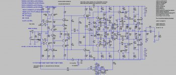
This is improved version of the lateral mosfet OPS with very similar technical data as previous version, but with DC servo outside the signal amplification path, very, very small sound impairment.
This amp looks complicate, with a lot of semiconductors used, but ones used in the signal amplification are not so many, it is in principle very simple schematic.
BR Damir
This amp looks complicate, with a lot of semiconductors used, but ones used in the signal amplification are not so many, it is in principle very simple schematic.
BR Damir
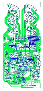
Attachments
Looks good to me, don't mind apparent complexity
I was straggling with the way how to implement DC servo with less on sound influence. Standard way to connect the DC servo is at the feedback point and not so good. I took idea from OS, I don't know if it was his design or he took it from some commercial amp, but it was eye opener when I saw it, it was so obvious, how I could not see it, what I missed was the ground connection.
Damir
Know what you mean, it is an obvious way of doing it when you see it. It is also has the advantage that it is not affected by using low resistor values in the feedback network.
I like this amp. It has a nice implementation of the CFA front end. May borrow (copy) it for the next prototype. Seems better than the classic diamond.
This is improved version of the lateral mosfet OPS with very similar technical data as previous version, but with DC servo outside the signal amplification path, very, very small sound impairment.
BR Damir
THx-RNMarsh
I was straggling with the way how to implement DC servo with less on sound influence. Standard way to connect the DC servo is at the feedback point and not so good. I took idea from OS, I don't know if it was his design or he took it from some commercial amp, but it was eye opener when I saw it, it was so obvious, how I could not see it, what I missed was the ground connection.
Damir
No , it was member Miib's idea of "floating" the IP pair with CM's ,
I just modified the CCS/servo FB arrangement.
NO commercial PA I know of does this.
Miib/OS servo "trick" .
OS
This is low power version I am going to build. I have two 80 W JLH amps with Hitachi laterals and I will use one and convert it to the CFA. I will use existing power supply and the box and this restrict the layout. It is very similar to the high power version.
BR Damir
BR Damir
Attachments
- Home
- Amplifiers
- Solid State
- 200W MOSFET CFA amp