Tube_Dude said:
What you mean by input stage balance???
That in the two colectors of the LTP pass the some current?
Yes, the two sides of each LTP have equal
current for minimum open loop distortion.
No, this only ocurrs when both LTPs are balanced since upper and lower bases are tied and current sources are of the same value
I'm sorry but as far as I can see both LTP's can be unbalanced
in the same direction, so Iq's are equal, I still cannot see how
each LTP is forced to be balanced.
As I said above slightly rephrased:
Its quite easy to build an amplifier with a single ended unbalanced LTP input, and it will quite happily still work, so why is this not possible with a double ended LTP input ?
") sreten.
sreten.sreten said:
I'm sorry but as far as I can see both LTP's can be unbalanced
in the same direction, so Iq's are equal, I still cannot see how
each LTP is forced to be balanced.
How both LTP could be unbalanced in the same direction?
Remember that upper lower bases are tied toghether, current sources are of the same value and transistors/resistors are matched by pairs like in a single ended LTP
To get noticeable unbalance in the same direction you need severely unmatched Vbe or resistors
[In a single ended LTP with a current mirror you would get severe offset in the same unmatched conditions]
Eva said:
How both LTP could be unbalanced in the same direction?
Remember that upper lower bases are tied toghether, current sources are of the same value and transistors/resistors are matched by pairs like in a single ended LTP
To get noticeable unbalance in the same direction you need severely unmatched Vbe or resistors
[In a single ended LTP with a current mirror you would get severe offset in the same unmatched conditions]
In real life very easily. Consider a single ended LTP driving a
VAS base-emitter to ground. Lets say Vbe of VAS = 0.7 volts.
Lets assume a LTP current of 2mA so Rc = 700R, 1mA per side.
(collector resistor only used on one side of the LTP)
A Rc of 1.4K will force a unbalance of 1.5mA/0.5mA and
this will force the Vbe's of the LTP pair to be different.
Nevertheless the amplifier will still function quite happily.
(With assymetric slewing and more DC offset and distortion).
sreten.Eva said:A balanced contribution to a little unbalanced world ...
slightly different numbers (multisim):
voltage drop upper collector resistor, voltage drop off lower collector resistor, and current through the VAS.
with no VAS emitter resistors: 728mv, 781mv, 30.8ma;
with 1ohm VAS emitter resistors: 752mv, 806mv, 27.8ma;
with 10ohm VAS emitter resistors: 853mv, 907mv, 14.7ma;
with 100ohm VAS emitter resistors: 938mv, 994mv, 2.8ma;
do you guys spot a problem?
I have no idea how the simulator calculated those numbers,
I will try two other simulators later.
millwood said:
slightly different numbers (multisim):
voltage drop upper collector resistor, voltage drop off lower collector resistor, and current through the VAS.
with no VAS emitter resistors: 728mv, 781mv, 30.8ma;
with 1ohm VAS emitter resistors: 752mv, 806mv, 27.8ma;
with 10ohm VAS emitter resistors: 853mv, 907mv, 14.7ma;
with 100ohm VAS emitter resistors: 938mv, 994mv, 2.8ma;
do you guys spot a problem?
I have no idea how the simulator calculated those numbers,
I will try two other simulators later.
The simulation is flawed as there are no base resistances which
allow Vbe differences to develop. With the circuit shown the the
left and right Vbe's must be equal, not the case in real life.
The circuit has no voltage input.
If Vbe's are equal then Ic must be equal as shown,
but this is putting the cart before the horse.
sreten.protel dxp didn't do much better: it wouldn't simulate when the VAS emitter resistor is 0ohm, complaining about singular matrix.
again, the same formate: upper collector resistor voltage drop, lower collector resistor voltage drop, and VAS collector current.
with 0.0001ohm VAS emitter resistor: 634mv, 1089mv (Wow!), and 12.55ma.
with 1ohm VAS emitter resistor: 643mv, 1098mv, 11.82ma.
with 10ohm VAS emitter resistor: 694mv, 1142mv, 7.73ma.
with 100ohm VAS emitter resistor: 760mv, 1195mv, 1.85ma.
BTW, all of them started to oscillate after about 15us, about 1 cycle per 0.1us (10mhz?).
sreten said:The simulation is flawed as there are no base resistances which
allow Vbe differences to develop. With the circuit shown the the
left and right Vbe's must be equal, not the case in real life.
The circuit has no voltage input.
If Vbe's are equal then Ic must be equal as shown,
but this is putting the cart before the horse.
not sure which base resistance you were talking about and which "left" and "right" you were talking about. It actually had a 10k resistor from the non-inverting end to the ground. and it does have a signal source (1vp, 1000hz).
the Vbe difference you saw (on the two resistors) are due to difference between npn and pnp devices.
I've realised one thing :
each LTP pair in the double ended circuit does not need
to be balanced, the double ended nature of the circuit will
cancel distortion the same way a single ended LTP pair
that is balanced will.
So my original comment about "input balance" is wrong,
the input is balanced, whether each LTP pair is irrelevant.
But the balance of each pair needs to be known to
know the VAS current, this balance and the VAS current
is still indeterminate, in that its not easily calculated.
I'm sure it is deterministic, but my maths aren't up to the job.
Enter a simulator, with all relevant circuit values.
What I am sure about is a Rc value gives a VAS current
and the current balance in each LTP pair, and that one
cannot easily calculate either without assumming one.
Unless I've missed something..........
sreten.
each LTP pair in the double ended circuit does not need
to be balanced, the double ended nature of the circuit will
cancel distortion the same way a single ended LTP pair
that is balanced will.
So my original comment about "input balance" is wrong,
the input is balanced, whether each LTP pair is irrelevant.
But the balance of each pair needs to be known to
know the VAS current, this balance and the VAS current
is still indeterminate, in that its not easily calculated.
I'm sure it is deterministic, but my maths aren't up to the job.
Enter a simulator, with all relevant circuit values.
What I am sure about is a Rc value gives a VAS current
and the current balance in each LTP pair, and that one
cannot easily calculate either without assumming one.
Unless I've missed something..........
sreten.millwood said:
not sure which base resistance you were talking about and which "left" and "right" you were talking about. It actually had a 10k resistor from the non-inverting end to the ground. and it does have a signal source (1vp, 1000hz).
the Vbe difference you saw (on the two resistors) are due to difference between npn and pnp devices.
In EVA's original circuit assuming output = ground (which must be
the theorectical case), each LTP pair bases summing horizontally
must have the same Vbe, (which is why Ic's are equal), and this
circuit has no voltage input, as it has no base resistances.
The value of Rc only determines the output current, theorectically.
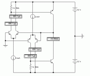
sreten.Attachments
now, from the LTspice (using ideal transistors):
with 0.0001ohm VAS emitter resistor: 850mv, 850mv, 14.6ma;
with 1ohm VAS emitte resistors: 850mv, 850mv, 13.5ma;
with 10ohm VAS emitter resistors: 910mv, 910mv, 8.1ma;
with 100ohm VAS emitter resistors: 980mv, 980mv, 1.8ma.
those readings are eye-balled so there might be some human errors but they should be small.
sreten said:
In EVA's original circuit assuming output = ground (which must be
the theorectical case),
that isn't assumed, it is given since the base of the left most npn transistor is tied to the ground, and the 2nd left most npn transistor is identical to the left most npn transistor so the base of the 2nd left most npn transistor, which happens to be the output, is tied to the ground.
sreten said:
each LTP pair bases summing horizontally
must have the same Vbe, (which is why Ic's are equal), and this
circuit has no voltage input, as it has no base resistances.
I don't understand the rest of the argument so I will leave it as is.
I think other than eva's simulation, all of mine are suggesting:
1) the collector current on the LTP is not evenly split within a given LTP; and Ic is not equal across two LTPs.
2) Ic of VAS seems to be very sensitive to Re of VAS. I am not sure why that's a good thing for mass-produced amps.
3) Ic of VAS declines as the VAS emitter resistor goes up. make intuitive sense.
4) none of the simulated results tie exactly but are all in the general ballpark. Probably due to slight difference in models used.
Still, I have no idea how the simulators come to the results. Any of your guys can calculate the collector current for the LTP and VAS? then show us your calculation.
wow... this discussion is still running...
and nobody tried the simulation using different transistors
(how about one small signal transitors and one power transistor
in the differential amp)..
come on... some more playing around ;-)
The symmetrical complementary design is definitely giving good
seld biasing, as long as equal shared currents of the differential stage allow enough voltage drop at some resitors to drive the
output stage (at least 0.7V drop at the resitors which give the voltage to drive the output stage). As Eva said even with emitter resitors in the output stage you will get a self biasing, but poor thermal behaviour of the current in the output stage.
If you place 33 Ohms at the four transitors of the differential stage and 100 Ohms at the emitters of the output stage,
giving 2mA in sum for each differential amp (sharing about 1mA/1mA *g*), and let one tail (on both sides) of the differential work with 1 kOhm to drive the output stage you will get a quite rugged thing that should also be able to deal with a mixture of 2n2222 and 2n3055!

Cheers
Markus
and nobody tried the simulation using different transistors
(how about one small signal transitors and one power transistor
in the differential amp)..
come on... some more playing around ;-)
The symmetrical complementary design is definitely giving good
seld biasing, as long as equal shared currents of the differential stage allow enough voltage drop at some resitors to drive the
output stage (at least 0.7V drop at the resitors which give the voltage to drive the output stage). As Eva said even with emitter resitors in the output stage you will get a self biasing, but poor thermal behaviour of the current in the output stage.
If you place 33 Ohms at the four transitors of the differential stage and 100 Ohms at the emitters of the output stage,
giving 2mA in sum for each differential amp (sharing about 1mA/1mA *g*), and let one tail (on both sides) of the differential work with 1 kOhm to drive the output stage you will get a quite rugged thing that should also be able to deal with a mixture of 2n2222 and 2n3055!
Cheers
Markus
..and the higher you set the values of the emitter resistors of the
differential amp the better will be the self biasing also with
unmatched transistors...
....OK, open loop gain will drop, but could be easily increased again
with paralleling capacitors to the emitter resistors.....
differential amp the better will be the self biasing also with
unmatched transistors...
....OK, open loop gain will drop, but could be easily increased again
with paralleling capacitors to the emitter resistors.....
millwood said:
I don't understand the rest of the argument so I will leave it as is.
I think other than eva's simulation, all of mine are suggesting:
Not a good idea to give results of a circuit not posted,
in a post that references a post that includes a circuit,
without explaining this is the case, JMO
, sreten.Showing my calculation:
Starting from the original 150W schematic...
The current sources with the red LED and a BJT + 470 Ohms
will make about 2.2 mA.
(assuming about 1.6V...1.7 across the LEDs and Ube of about 0.6V for the transitors...)
The differential amp is put directly to ground at the right side.
The left side is getting the signal zero from feedback and no input.
So both inputs are on the voltage.
So the voltage from the base of both NPN + emitter resitors to the current source is equal (Ube_left+Ure_left = Ube_right+Ure_right).
The same in PNPs.....
If the current tends to share unbalanced then the path with the lower current will show a lower voltage drop across the resitor==> more voltage for the basis emitter==> stabillizing effect to reduce the unbalance.
Going on we might have 1.1mA in each tail (just an estimation
up to now...) we would have 748mV across R9 and R10.
Minus about 0.6V across Ube of T7 (same in T8) we will find about
148mV across R15 and R16 ==> making about 3mA through
T7 and T8, symmetrical ==> resulting in an ouptut close to ground... this output is feed back to the left side of the differential amp
==> loop closed ==> operating point stable.
Now lets estimate one unmatched transitor, say T1 may only have
Ube of 550mV....
Then T1 would get more current than T2.
Less current in T2 means less drive for T7 ==> the output will go to negative values ==> this negative output is feed back to the left side of the differential amp and is reducing the current through
T1 ===> self stabillzing behaviour..
Enjoy the night
Markus
ChocoHolic said:Showing my calculation:
Markus
let's not start with the original schematic as we have no measured nor simulated results: anyone can come up with a set of numbers and we woul dhave no way of knowing how accurate / correct those numbers are.
Start with the schematic that EVA had posted and I had simulated against, and show your results.
...I am nearly in bed....
OK with EVA's schematic.
I would like to add emitter resitors (100 Ohms) to the output stage, otherwise the current of the output stage will depend very much on the transistors, which I cannot calculate in mind.
(FYI: This heavy influence of the transistor characteristic and
the thermal behaviour is exactly the reason why professional
mass products have these resistors)
The differential amp can remain without emitter resistors.
OK.
Currents sources with 2mA.
Left side of differential amps on ground.
Right side estimated also at ground level (no input signal
steady state point).
The Ube of both NPN is the same (both basis at ground and emitters
connected together). If transistors are matched and have the same Ube then the current in both tails will split balanced.
The same with the NPNs.
Going on with this estimation we will have about 1mA in each tail (In my mind I would simply neglect the 10µA current of the basis...).
1mA at 1k Ohm will make 1V .
This 1V minus about 0.6V will be seen across the emitter resistors of the output stage. The upper transistor will make 4 mA.
The lower one the same. Their collectors will be close to ground.
This zero signal is feed back to the right side of the differential amps
as already assumed above.
Everything is matching together with the closed loop.
Now let's try to unbalance.
May be the left NPN would have a lower Ube than the right NPN.
Then the left NPN would make a higher current than the right NPN.
This would make more base drive for the upper transistor of the output stage. This now would pull the output to the positive.
This positive signal is feed back to the right side of the differential amps. If the right side is pulled up then the current in the left transistor will decrease ==> stabilizing aginst the origin of unbalance...
Bye
Markus
- Status
- This old topic is closed. If you want to reopen this topic, contact a moderator using the "Report Post" button.
- Home
- Amplifiers
- Solid State
- 150W Is it good?