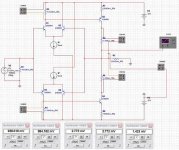
taking sreten's advice, I am posting the schematic I simulated in multisim. here it is.
not much of a difference, other than that I used an input resistor, and an output resistor. the key thing that I didn't measure until after reading one of sreten's earlier posts is the output offset. As you can see, there is a 1.4mv positive offset on the inverting ends of the LTPs.
edit: wanted to add that if I change R1 to 0ohm, and R3 to 22meg (effectively EVA's schematic), I get the same readings.
edit 2: DC offset is:
with 0ohm VAS emitter resistors: -217uv;
with 1ohm VAS emitter resistors: 31uv;
with 10ohm VAS emitter resistors: 910uv.
with 100ohm VAS emitter resistors: 1.423mv.
while the bases of non-invernting ends are firmly tied to 0v / ground.
Attachments
So what voltage gain do you get with R1 = 0ohm ?
And V3 has an output voltage ?
(How does your simulator deal with the quandary ?
V3 = 0 ? or V3 = V3 ? )
Its not a good idea to ask simulators such questions.
(In Eva's original circuit the LTP pairs are forced to
be current mirrors as Vbe's have to be equal. Not
the real case.)
") sreten.
sreten.
And V3 has an output voltage ?
(How does your simulator deal with the quandary ?
V3 = 0 ? or V3 = V3 ? )
Its not a good idea to ask simulators such questions.
(In Eva's original circuit the LTP pairs are forced to
be current mirrors as Vbe's have to be equal. Not
the real case.)
sreten.sreten said:So what voltage gain do you get with R1 = 0ohm ?
And V3 has an output voltage ?
only if you could figure out how to drive such a load,
sreten said:(How does your simulator deal with the quandary ?
V3 = 0 ? or V3 = V3 ? )
?
ChocoHolic said:...I am nearly in bed....Markus
I feel for you.
ChocoHolic said:Right side estimated also at ground level (no input signal
steady state point).Markus
maybe that's where the problem comes from,
the whole thing may work like this:
the system will change the DC offset. the DC offset will also change current on the two collector resistors: higher DC offset will decrease the current going through the upper collector resistor (R2) and increase the current going through the lower collector resistor. As voltage drop off R2 goes down, Q3 opens up less and decreases the DC offset.
the process stops until the two VAS transistors reach about the same collector current. and the DC offset will then settle.
the currents are likely to dependent on device characteristics more than resistor values -> not good for manufacturing.
on the other hand, the process appears to be thermally stable: a decline in Q3's Vbe will increase its collector current, which increass the DC offset. that in turn will lower voltage drop off R2 to compensate for the Vbe drop on Q3.
thanh said:why don't you add resistors collector of Q2 Q6
As the colectors of Q2 and Q6 are not used ...to add resistors doesn't change anything..
I've given the whole thing some thought and concluded the following :
For the double ended LTP and emitter degenerated VAS you
choose your design currents. You then calculate the base voltage
of the VAS asumming the design current of the VAS and use this
and 1/2 the LTP current to set the LTP collector resistor.
You then connect them together, the results
will be near design values, hopefully.
Compared to a single ended LTP and VAS :
Each LTP pair cannot be balanced as accurately, but exact
balance is not needed as the double ended nature of the
circuit (which is balanced) cancels distortion the same way
a near exactly balanced single ended LTP does.
Given the balance of each LTP pair is not exact the actual VAS
current is not exact, it cannot be set as accurately / predictably
as in the single ended case.
This on its own is not a big deal, but the thermal stability of
the VAS current may be depending the biasing scheme used.
sreten.
For the double ended LTP and emitter degenerated VAS you
choose your design currents. You then calculate the base voltage
of the VAS asumming the design current of the VAS and use this
and 1/2 the LTP current to set the LTP collector resistor.
You then connect them together, the results
will be near design values, hopefully.
Compared to a single ended LTP and VAS :
Each LTP pair cannot be balanced as accurately, but exact
balance is not needed as the double ended nature of the
circuit (which is balanced) cancels distortion the same way
a near exactly balanced single ended LTP does.
Given the balance of each LTP pair is not exact the actual VAS
current is not exact, it cannot be set as accurately / predictably
as in the single ended case.
This on its own is not a big deal, but the thermal stability of
the VAS current may be depending the biasing scheme used.
sreten.What about adding a schottky diode in series with the base resistor of the VAS?
For so lower currents the schottky may be dropping only .15 to .20V
Schottky diodes also have negative temperature coefficient on junction potential and after looking at some curves I think it may be enough to compensate the negative coefficient on the Vbe of the VAS
I have to try it ... [had some small 1A schottkys lying around]
sreten, I think you are right. The whole doesn't seem to be as calculatable as single LTP/VAS. I wonder how much variance there is in production amps using complementory ltp/vas.
thermal stability is not a problem as the VAS current drops when Vbe of VAS transistors drops. so it is self-stabilizing.
what I observed is that there are always about 200mv of voltage drops on the degenerate resistors for VAS. Not sure what caused it but it is pretty consistent. it may be a useful thing is setting up this circuitry.
Hi Sreten, All,
I also had this impression, but running LTSpice for temperatures from 15 to 40 degrees Celcius gave less than 15% change. Not really problematic, I assume.
I'd suggest some other points should be looked at:
- If you aren't pretty sure about your signal source, perhaps a follower should be put before the input, so that the current summing works exactly.
- Output stage: no comments on my post #69?
http://www.diyaudio.com/forums/showthread.php?postid=326152#post326152
Regards,
Peter Jacobi
sreten said:[...]
Given the balance of each LTP pair is not exact the actual VAS
current is not exact, it cannot be set as accurately / predictably
as in the single ended case.
This on its own is not a big deal, but the thermal stability of
the VAS current may be depending the biasing scheme used.
[...]
I also had this impression, but running LTSpice for temperatures from 15 to 40 degrees Celcius gave less than 15% change. Not really problematic, I assume.
I'd suggest some other points should be looked at:
- If you aren't pretty sure about your signal source, perhaps a follower should be put before the input, so that the current summing works exactly.
- Output stage: no comments on my post #69?
http://www.diyaudio.com/forums/showthread.php?postid=326152#post326152
Regards,
Peter Jacobi
pjacobi said:- Output stage: no comments on my post #69?
http://www.diyaudio.com/forums/showthread.php?postid=326152#post326152
Regards,
Peter Jacobi
that's the famous T-circuitry. Leach used it in his design based on various simulations, but he offered no explanations.
I have simulated quite a few driver designs and found the T is always the winner. If someone can explain that I am all ears.
the cap is there to reduce switching distortion.
edit: I will offer one conjecture: the drivers in the T remain in class A throughout the cycle. they never switch off, unlike drivers in the traditional circuitry. but I am not sure how much of a big difference cross-over distortions at small signal levels will be.
My thoughts about the output stage :
The "T" circuit [drivers without connection to the output] produces consistent and fast turn-on/turn-off to the output devices, allows the drivers and pre-drivers to work in full class-A and reduces THD but at the expense of increasing current gain of the output stage and reducing phase margin
In the straightforward circuit [all transistors tied to the output], the drivers and the output devices are degenerated through its emitter resistors, having lower gain and providing more phase margin at the expense of class AB operation of the drivers and pre-drivers, higher THD and slower turn-on/turn-off of the output devices
[Wonders are also said about CFPs, but what happens when you drive a CFP into clipping at 20Khz?... When the output reaches the higher rail the lower devices may be still 'trying' to turn off... ]
]
The "T" circuit [drivers without connection to the output] produces consistent and fast turn-on/turn-off to the output devices, allows the drivers and pre-drivers to work in full class-A and reduces THD but at the expense of increasing current gain of the output stage and reducing phase margin
In the straightforward circuit [all transistors tied to the output], the drivers and the output devices are degenerated through its emitter resistors, having lower gain and providing more phase margin at the expense of class AB operation of the drivers and pre-drivers, higher THD and slower turn-on/turn-off of the output devices
[Wonders are also said about CFPs, but what happens when you drive a CFP into clipping at 20Khz?... When the output reaches the higher rail the lower devices may be still 'trying' to turn off...
]- Status
- This old topic is closed. If you want to reopen this topic, contact a moderator using the "Report Post" button.
- Home
- Amplifiers
- Solid State
- 150W Is it good?