I'm sorry TD but you got this one wrong.
You cannot assume the LTP's are balanced.
Your basic electronics in this case are too basic.
My original point is the LTP's are almost certainly not perfectly
balanced and the VAS current is not exactly known, because
circuit values cannot be easily defined.
Assume a VAS current say 30mA with 47R.
Work backwards and this will give you an unbalanced
LTP with too much current in the collector resistor side.
You can now adjust the collector resistor to give balance again.
But note you started by assuming a current, the only way you
can set the current is by assuming balance, and you cannot
do this as the above example shows.
Your calculations assume the collector resistor is the right value
to give balance, and from this you have derived the operational
points of the circuit.
But you can derive another set of operational points by assuming
a percentage + or - imbalance.
") sreten.
sreten.
You cannot assume the LTP's are balanced.
Your basic electronics in this case are too basic.
My original point is the LTP's are almost certainly not perfectly
balanced and the VAS current is not exactly known, because
circuit values cannot be easily defined.
Assume a VAS current say 30mA with 47R.
Work backwards and this will give you an unbalanced
LTP with too much current in the collector resistor side.
You can now adjust the collector resistor to give balance again.
But note you started by assuming a current, the only way you
can set the current is by assuming balance, and you cannot
do this as the above example shows.
Your calculations assume the collector resistor is the right value
to give balance, and from this you have derived the operational
points of the circuit.
But you can derive another set of operational points by assuming
a percentage + or - imbalance.
sreten.millwood said:
In a typical ltp (with resistors), the current in each arm is determined by the VAS stage. So you would know the voltage drop off R15, plus the Vbe of T7. then you can calculate the current through the 680ohm resistor for T2.
In this case, there is no way to determine the voltage drop off the 680ohm resistor, nor the idle current for the VAS.
Sorry to say...but what you are saying is not correct...do some readings about the subject.
I don't want to repeat my self...i have done the calculation you have asked...and you can be sure that they are correct.
Have you any other values?...Of your calculation!!
ChocoHolic said:Hi folks!
I think Dude is right.
Depending on 47 Ohms or 100 Ohms I also end
up in about 10mA (100 Ohms) or 20mA (47 Ohms).
Thanks Markus...after all is a very easy calculation!!!
...well they will be more or less balanced, let's says less than
15% mismatch.
But I have to correct my values.
Red LEDs typically show a voltage drop around 1.8V (if I remember right), not 2.8V.... Coming from this we will have about 1. 2 mA in each tail. Multiplied with 680 Ohms ==> 816mV minus Ube about 200mV across the resitor.... 47 Ohms should be OK without frying the transistors....
Tube_Dude said:Have you any other values?...Of your calculation!!
I cannot calculate it, because it is not calculatable as sreten has pointed out, unless you wanted me to calculate it incorrectly,
millwood said:
edit: tube-dude, you may wan tto look into this thread to better understand the issue here.
http://www.diyaudio.com/forums/showthread.php?s=&threadid=16796
In the first schematic of the link you gave the VAS current is not perfectely defined because the VAS transistor doesn't have emmiter degeneration (resistor)..
ChocoHolic said:...well they will be more or less balanced, let's says less than
15% mismatch.
But I have to correct my values.
Red LEDs typically show a voltage drop around 1.8V (if I remember right), not 2.8V.... Coming from this we will have about 1. 2 mA in each tail. Multiplied with 680 Ohms ==> 816mV minus Ube about 200mV across the resitor.... 47 Ohms should be OK without frying the transistors....
Hi Markus...
2,8 volts was a arbitrary value that millwood gave us...only for calculation.
Tube_Dude said:
In the first schematic of the link you gave the VAS current is not perfectely defined because the VAS transistor doesn't have emmiter degeneration (resistor)..
if you are talking about Q18 on the upper side: if it had a emitter resistor, you would not have been able to calculate the current on R17.
the problem with that circuit is that while the current and voltage on the current mirror are determined, the current going through Q18 isn't determinate.
much like the 2nd half of our problem here.
Tube_Dude said:
In the first schematic of the link you gave the VAS current is not perfectely defined because the VAS transistor doesn't have emmiter degeneration (resistor)..
In a non balanced circuit, one LTP and one VAS transistor the
VAS current is set by a current source. The non degenerated
base emitter is treated as a Vbe volt drop virtual earth.
This allows you to set the collector resistor/ current by assuming
a Vbe drop across the resistor, the resistor is set to give current
balance in the LTP.
As the VAS current is known, degenerating the VAS transistor
doesn't cause any problems in balancing the LTP, the extra
drop across the emitter resistor just needs accounting for.
You cannot do this in the balanced 2 LTP's and 2 VAS Tr's case.
sreten.millwood said:
if you are talking about Q18 on the upper side: if it had a emitter resistor, you would not have been able to calculate the current on R17.
the problem with that circuit is that while the current and voltage on the current mirror are determined, the current going through Q18 isn't determinate.
much like the 2nd half of our problem here.
In the problem of the link the VAS is drived by a high impedance point (connection of colector of Q1 and Q6)...only in this case the voltage at this point is defined by the current in the VAS.
In our case the resistor has 680 Ohms and the input of the VAS with a current gain of say 100 will be 10KOhms with 100 Ohms emiter resistor
So the resistor voltage define the operation point of the VAS and consequently the current in the VAS.
ChocoHolic said:...well they will be more or less balanced, let's says less than
15% mismatch.
depending on what "mismatch" we are talking about here. if it is Vbe mismatch, because of high hfe of those small signal transistors, the Ic variation from 15% Vbe mismatch can be tremendous.
if you are talking about hfe mismatch, then you will need to know the base current. which is in turn determined by base voltages at the inverting and non-inverting input transistors, and their respective Vbe thresholds.
In general, you cannot assume that the tail current will be equally split.
The tail current is near perfectly split because the emiters of the LTP are drived by a high impedance , megaohms(the colector of the CCS) so the emiters are current drived and then the Vbe of the transistors doesn't matter...millwood said:
depending on what "mismatch" we are talking about here. if it is Vbe mismatch, because of high hfe of those small signal transistors, the Ic variation from 15% Vbe mismatch can be tremendous.
if you are talking about hfe mismatch, then you will need to know the base current. which is in turn determined by base voltages at the inverting and non-inverting input transistors, and their respective Vbe thresholds.
In general, you cannot assume that the tail current will be equally split.
Hi Millwood,
I was talking about the mismatch of the DC-current
in the tails of the differential amplifiers.
The emitter resistors with about 30 Ohms will results
in acceptable balancing.
One end of the differential amps is having OV signal.
The feedback will give also nearly around 0V back to
the other input. ==> Both inputs of the differential amps
at 0V. Emitters connected via 30 Ohms together, why do
expect an uncaculatable behaviour or heavy mismatch
in current sharing?
The schematic in the other thread is just another thing.
T14 and T18 had no emitter resistors and a to small
bias voltage to drive them.....
It was solved by increasing the driving voltage (values of R16 and R17 increased) and additional emitter resitors......
In our circuit we have about 0.8V to drive T7 and T8 plus their
emitter resistors. About 150-200mV across this emitter resistors is not much, but should give acceptable thermal behaviour.
What's the problem? I simply cannot get your point....
Cheers
Markus
Cheers
Markus
It's important to distinguish between Signle-Ended Long-Tailed-Pair and complimentary LTPs
In SE LTP the most common practice is to load the Voltage Amplifier Stage with a current source. This current source is what determines VAS biasing and thus SE LTPs have to be designed to provide, without imbalances, the drive current needed by the VAS to reach its biasing point. A common practice is to use current mirrors since they are simple to implement and almost guarantee balance, but selecting the right resistors and currents does also the job
Complimentary LTPs with complimentary VAS are tricky since the biasing in the VAS is fully dependent on the biasing of the LTPs. Current mirrors are very hard to implement in this case since they don't provide any reliable fixed biasing to the VAS by themselves. The most common solution in this case is to carefully select resistors and currents in a way that guarantees reliable biasing
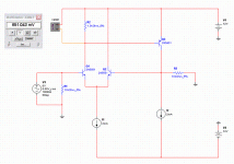
Let's analyze the circuit we are discussing :
Assuming 2V drop in the LEDs and 700mV Vbe in the current source transistors, we have (2-.7)/470=2.76mA of total biasing for each LTP, assuming the current source in the low rail has been adjusted to match the other one
The theoretical AC low frequency current gain in the VAS [excluding miller capacitor effects] is the ratio between base and emitter resistors : 680 / 47 = 14.47
Assuming 680mV Vbe in the VAS transistors, the minimum current needed to turn on the VAS is .680/680 = 1mA
So the bias current in the VAS is equal to : (LTP-leg-current - 1mA) * 14.47
Assuming an ideal output stage and upper and lower VAS with identycal properties, then there is a unique balance point that is reached when both VAS have the same current output and thus the same current input
Looking at the circuit, it can be easily seen that output currents of the LTPs are complimentary so the balance will be reached when these currents are equal
Assuming matched transistors and resistors in each LTP side, output currents in both sides only could be equal when both legs are balanced, since when upper current increases the other decreases
So in the end, assuming ideal identycal transistors and resistors we must have 2.76/2 = 1.38mA in each leg of each LTP
And with 1.38mA, the VAS is biased at : (1.38-1)*14.47 = 5.5 mA
In the real world, sources of imbalance in each LTP would be :
1 - Mismatching of Vbe of LTP transistors and value of resistors, so matching within each pair is a great idea
2 - Different Vbe for NPN and PNP VAS and VAS resistor mismatching : This is cured using the trimmer in the lower current source to increase or reduce the biasing current of the higher LTP until optimum balance is reached [One LTP will allways end with different biasing than the other, but legs within each LTP will be balanced]
3 - Different beta and Vbe in the output stages : The trimmer also does that job
Null offset point is more tricky since it may not coincide with best LTP balance point. It depends on upper LTP and lower LTP Ib cancellation so it would be a great idea to beta-match if possible the upper and lower transistors of the left leg of the LTPs. The beta of the transistors in the right leg is unimportant since its bases are grounded
I would use 33K and 1K instead of 330K and 10K since it will lower noise and reduce offset. To drive this 1K input impedance I would place a simple op-amp and at the same time I would use it as a balanced input [I like balanced interconnect]
Dissipation in each VAS is : 5.5mA * 60V = 330mW and Rth_jc for TO-92 is 233ºC/W so temp. increase would be about 75ºC and junction temperature would be 100ºC at 25ºC ambient temperature, a little hot to my taste
Using 100 ohms emitter resistors will reduce biasing and heating to the half, but I think 2.75mA is too little biasing. A better alternative would be to use two 2N5401/5551 with independent 100 ohm emitter resistors, and with bases and collectors paralelled
As for the complimentary LTPs with current mirrors, the only way I've found to make it work is using an optocoupler to sense VAS biasing [photo-led in series with the collector of the Vbe multiplier] and use it with some adittional transistors to inject/rob current on the outputs of the current mirrors [as some kind of servo-bias-control]
In SE LTP the most common practice is to load the Voltage Amplifier Stage with a current source. This current source is what determines VAS biasing and thus SE LTPs have to be designed to provide, without imbalances, the drive current needed by the VAS to reach its biasing point. A common practice is to use current mirrors since they are simple to implement and almost guarantee balance, but selecting the right resistors and currents does also the job
Complimentary LTPs with complimentary VAS are tricky since the biasing in the VAS is fully dependent on the biasing of the LTPs. Current mirrors are very hard to implement in this case since they don't provide any reliable fixed biasing to the VAS by themselves. The most common solution in this case is to carefully select resistors and currents in a way that guarantees reliable biasing
Let's analyze the circuit we are discussing :
Assuming 2V drop in the LEDs and 700mV Vbe in the current source transistors, we have (2-.7)/470=2.76mA of total biasing for each LTP, assuming the current source in the low rail has been adjusted to match the other one
The theoretical AC low frequency current gain in the VAS [excluding miller capacitor effects] is the ratio between base and emitter resistors : 680 / 47 = 14.47
Assuming 680mV Vbe in the VAS transistors, the minimum current needed to turn on the VAS is .680/680 = 1mA
So the bias current in the VAS is equal to : (LTP-leg-current - 1mA) * 14.47
Assuming an ideal output stage and upper and lower VAS with identycal properties, then there is a unique balance point that is reached when both VAS have the same current output and thus the same current input
Looking at the circuit, it can be easily seen that output currents of the LTPs are complimentary so the balance will be reached when these currents are equal
Assuming matched transistors and resistors in each LTP side, output currents in both sides only could be equal when both legs are balanced, since when upper current increases the other decreases
So in the end, assuming ideal identycal transistors and resistors we must have 2.76/2 = 1.38mA in each leg of each LTP
And with 1.38mA, the VAS is biased at : (1.38-1)*14.47 = 5.5 mA
In the real world, sources of imbalance in each LTP would be :
1 - Mismatching of Vbe of LTP transistors and value of resistors, so matching within each pair is a great idea
2 - Different Vbe for NPN and PNP VAS and VAS resistor mismatching : This is cured using the trimmer in the lower current source to increase or reduce the biasing current of the higher LTP until optimum balance is reached [One LTP will allways end with different biasing than the other, but legs within each LTP will be balanced]
3 - Different beta and Vbe in the output stages : The trimmer also does that job
Null offset point is more tricky since it may not coincide with best LTP balance point. It depends on upper LTP and lower LTP Ib cancellation so it would be a great idea to beta-match if possible the upper and lower transistors of the left leg of the LTPs. The beta of the transistors in the right leg is unimportant since its bases are grounded
I would use 33K and 1K instead of 330K and 10K since it will lower noise and reduce offset. To drive this 1K input impedance I would place a simple op-amp and at the same time I would use it as a balanced input [I like balanced interconnect]
Dissipation in each VAS is : 5.5mA * 60V = 330mW and Rth_jc for TO-92 is 233ºC/W so temp. increase would be about 75ºC and junction temperature would be 100ºC at 25ºC ambient temperature, a little hot to my taste
Using 100 ohms emitter resistors will reduce biasing and heating to the half, but I think 2.75mA is too little biasing. A better alternative would be to use two 2N5401/5551 with independent 100 ohm emitter resistors, and with bases and collectors paralelled
As for the complimentary LTPs with current mirrors, the only way I've found to make it work is using an optocoupler to sense VAS biasing [photo-led in series with the collector of the Vbe multiplier] and use it with some adittional transistors to inject/rob current on the outputs of the current mirrors [as some kind of servo-bias-control]
since I cannot convince you, so here is a simulation. I minimized the number of variables to make it as silmple as possible.
notice the voltage drop off R2? how much current is going through R2 vs. the tail current?
note that you have perfectly matched transistors here.
I can also tell you that (within a range), the voltage drop off R2 is indepdent of the value of R2. Why is that?
hope this helps.
notice the voltage drop off R2? how much current is going through R2 vs. the tail current?
note that you have perfectly matched transistors here.
I can also tell you that (within a range), the voltage drop off R2 is indepdent of the value of R2. Why is that?
hope this helps.
Attachments
millwood said:
I can also tell you that (within a range), the voltage drop off R2 is indepdent of the value of R2. Why is that?
Because the down side of R2 is keped fixed a one diode drop from the + rail...you forget the emitter resistor...
ChocoHolic said:I was talking about the mismatch of the DC-current
in the tails of the differential amplifiers.
The emitter resistors with about 30 Ohms will results
in acceptable balancing.
One end of the differential amps is having OV signal.
The feedback will give also nearly around 0V back to
the other input. ==> Both inputs of the differential amps
at 0V. Emitters connected via 30 Ohms together, why do
expect an uncaculatable behaviour or heavy mismatch
in current sharing?
Markus
the emitter resistors will sure help reduce mismatch in two transistors. However, it will NOT determine how much current going through each collector, as large variations in collector current can be reflected in only small voltage variance on the two bases.
the only thing we know of about LTP is that the current on the two collectors sums to (near) total current on the emitter (or CCS in my simulation).
Other than that, we cannot really rely on anything.
ChocoHolic said:Hi Millwood!
In your new schematic you will always have 0.6mA...0.7mA through
Q1 as the voltage across R2 is defined by be of Q3.
precisely. and sreten and I both pointed out earlier that the VAS will determine current in each arm of a LTP pair. and there is no assurance that the current in each arm is 50% of the tail current.
Now, going back to the schematic in question. because of its fully complementory nature of the circuitry, there is no current source to load up Q3, and worse yet, there is a degenerator in Q3's emitter. since we don't know how much current is going through Q3, we cannot calculate the voltage drop off R2 -> thus sreten's comment about the current on R2 indeterminate.
edit: actually the current going through Q1 can be adjusted by changing the value of R2. But that's a minor point.
- Status
- This old topic is closed. If you want to reopen this topic, contact a moderator using the "Report Post" button.
- Home
- Amplifiers
- Solid State
- 150W Is it good?