is 2sc2240 a good replacement for bc546?
2SC2240
Collector/base voltage VCBO 120 V
Collector/emitter voltage VCEO 120 V
Emitter/base voltage VEBO 5V
DC Current Gain HFE 200-700
BC546
Collector/Emitter Voltage 65V
Collector/Base Voltage 80 V
Emitter/Base Voltage 6.0 Vdc
DC Current Gain HFE 110-450
lastly here is a better layout of my fx8
How did you go with this layout? Did you get some made?
Sent from my HUAWEI MT7-L09 using Tapatalk

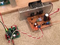
In my Preamp I am getting large DC offset of -900mV. I matched the input LTPs as before. Is there something else that should have been matched or can a pot be added somewhere to trim this. I bypassed the pot on the layout as that was for bias adjustment when running as an amp.
I am following Still4given's markups on an older PCB layout and using BD139/140's rather than BC639/640's per the Apex schematic.
Here were the modifications in red by Still4given that I had to implement in the slightly different layout I used.
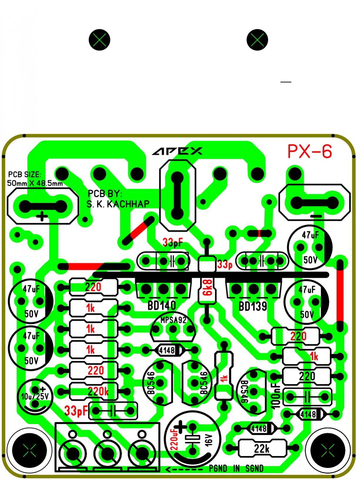
I am following Still4given's markups on an older PCB layout and using BD139/140's rather than BC639/640's per the Apex schematic.
Here were the modifications in red by Still4given that I had to implement in the slightly different layout I used.
Last edited:
The input LTP should be reasonably matched for hFE and Vbe, both measured at the operating current, they see in the circuit.
The base inputs both draw in a current =Ie/hFE
That input current causes a voltage drop on the biasing resistors at the +IN and -IN inputs.
You have an Ie ~1.5mA and assuming an hFE of 200, then Ib ~ 7.5uA
+IN sees 220k and drops 1.65V
-IN sees 6k8 and drops 51mV
The output offset is ~ -1.65V+51mV = -1.6V
If I now assume an hFE of ~350, then the calculated offset becomes ~900mV
The rule for opamp and it applies to this circuit as well is:
The NFB adjusts the output to eventually make the difference between the +IN and -IN as near zero as possible.
Use this to apply 900mV to the output and calculate to find the voltage at the -IN emitter.
Repeat to find the voltage at the +IN emitter. These should be equal.
Doing these two sets of calculations shows the effect of changing hFE and Vbe for the two sides of the LTP.
Last edited:
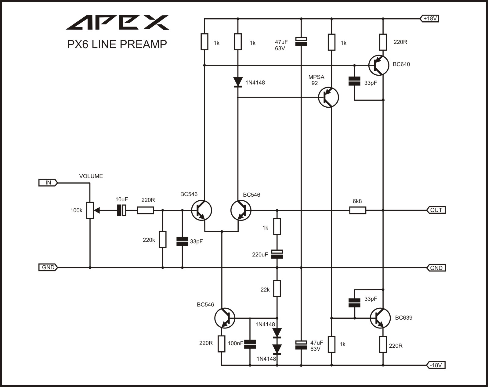
The low values of feedback resistors on this preamp are to maintain a low level of noise at the output.
It is this low -IN resistance that is giving the output offset.
I see four methods to improve that:
a.) adopt the Dr Cherry style of LF corrected feedback (using 2times 6k8 in series with the 6k8 and then parallel that 13k6 with a big electrolytic)
b.) adopt jFET LTP.
c.) Do both of the above and change the vol pot to 10k and the 220k becomes 20k
d.) increase the NFB values to match the +IN side.
Last edited:
I have lots of 2sk170's but they are not matched. I have not yet installed a volume pot - is that a problem with not loading the input resistance lower? The dr cherry seems interesting but how big of an electrolytic?
Is there me a pot I can put in place where NFB is to adjust offset? Or perhaps pot in series with one of LTP resistors to balance?
Despite this, when AC coupled the preamp sounds very good - like it wasn't there but with gain. Not bad for $2 in parts.
Is there me a pot I can put in place where NFB is to adjust offset? Or perhaps pot in series with one of LTP resistors to balance?
Despite this, when AC coupled the preamp sounds very good - like it wasn't there but with gain. Not bad for $2 in parts.
But I still can't design amplifiers.
that is weird Andrew you have plenty of knowledge , maybe one day you will make your own, why not ? you have a solid foundation,
I only know little

Regards
Juan
Last edited:
A gift from me. Not tested!
Hi Bimo,
Here is slightly modified layout of your version. I wanted to make space for inductor on PCB itself + some common cap sizes+ TO-126/220 Heat sink easily available . Would be nice if you could comment on the same.
reg
Prasi
Attachments
Last edited:
Hi Bimo,
Here is slightly modified layout of your version. I wanted to make space for inductor on PCB itself + some common cap sizes+ TO-126/220 Heat sink easily available . Would be nice if you could comment on the same.
reg
Prasi
Is Q2 and Q4 too close with heatsink?
Is Q2 and Q4 too close with heatsink?
yes. They can be moved away. I will do that, by moving them slightly below. thanks.
reg
prasi
I would suggest this cap for C4. Prasi can accommodate the leads and dia size for this?
UES0J102MHM1TO Nichicon | Capacitors | DigiKey
UES0J102MHM1TO Nichicon | Capacitors | DigiKey
If any of you object. I suggest make the DC caps 12.5mm with leads 5mm for C9,C12,C15,C16,
1) Boosting the uF can possibly aid in the bass with the 16mOhms ESR.
http://www.digikey.com/product-detai...2402-ND/613763
2) For C4:
Use this cap:
UES0J102MHM1TO Nichicon | Capacitors | DigiKey
Make the dia size to be 12.5mm and the lead space 5mm.
1) Boosting the uF can possibly aid in the bass with the 16mOhms ESR.
http://www.digikey.com/product-detai...2402-ND/613763
2) For C4:
Use this cap:
UES0J102MHM1TO Nichicon | Capacitors | DigiKey
Make the dia size to be 12.5mm and the lead space 5mm.
If any of you object. I suggest make the DC caps 12.5mm with leads 5mm for C9,C12,C15,C16,
1) Boosting the uF can possibly aid in the bass with the 16mOhms ESR.
http://www.digikey.com/product-detai...2402-ND/613763
2) For C4:
Use this cap:
UES0J102MHM1TO Nichicon | Capacitors | DigiKey
Make the dia size to be 12.5mm and the lead space 5mm.
Hi,
Already made changes (used 13mm dia x 5mm pitch). Will post after fine tuning the layout a bit.
reg
Prasi
Your link doesn't work:
http://www.digikey.com/product-detai...2402-ND/613763
http://www.digikey.com/product-detai...2402-ND/613763
Does the PX6 preamp operate in class A or AB?
PX6 preamp operate in class A
- Home
- Amplifiers
- Solid State
- 100W Ultimate Fidelity Amplifier