... Nulling DC offset / P2 functions flawlessly on both channels....
By this you mean that if you measure the voltage on the output you get some hundreds of mV, but by adjusting P2 you can get it under a couple of mV?
(And conversely, that by *un-adjusting* P2 you can get the output offset back to some hundreds of mV?)
If so, are you sure you're measuring the voltage across the source resistors right? The voltage that appears on your output had to come from somewhere. The only other alternative is D1/D2. Are you sure they're in the right way round?
Cheers,
Jeff.
Can you check if the voltage to the mosfet gates os moving as P1 changes?
You can just measure say with one probe at the end where R8 meets the gate resistors R10/R11/R12 and the other probe at where P1 meets R13/R14/R15? Does this
voltage change when you adjust P1?
What resistor value are you using for R8?
You can just measure say with one probe at the end where R8 meets the gate resistors R10/R11/R12 and the other probe at where P1 meets R13/R14/R15? Does this
voltage change when you adjust P1?
What resistor value are you using for R8?
Is this Ok..
Is the value of R3 correct?
if rails are there , DC offset is so-so , but you can't set Iq properly - measure which range of voltages you can get across bias voltage generator - practically measure voltages between upper and lower gates , while fiddling with trimpot at TL431
write here what you got
keep meter at DC offset position , same as second one across (any) source resistor , for Iq
also post here actual schematic , so we know that we are on same page
write here what you got
keep meter at DC offset position , same as second one across (any) source resistor , for Iq
also post here actual schematic , so we know that we are on same page
By this you mean that if you measure the voltage on the output you get some hundreds of mV, but by adjusting P2 you can get it under a couple of mV?
(And conversely, that by *un-adjusting* P2 you can get the output offset back to some hundreds of mV?)
Correct. I started out at just over 150mV or so on each channel. I can dial it down to essentially 0 and go negative also.
If so, are you sure you're measuring the voltage across the source resistors right? The voltage that appears on your output had to come from somewhere. The only other alternative is D1/D2. Are you sure they're in the right way round?
Cheers,
Jeff.
Checked D1 and D2 on both sides. They are oriented correctly. I thought the same thing re: measuring properly. Usually that's the culprit
 I am simply measuring across the source resistors. R16 through R21. 0V on all of them with different DMMs. I am missing something painfully obvious.
Can you check if the voltage to the mosfet gates os moving as P1 changes?
You can just measure say with one probe at the end where R8 meets the gate resistors R10/R11/R12 and the other probe at where P1 meets R13/R14/R15? Does this
voltage change when you adjust P1?
What resistor value are you using for R8?
Thank you for this idea. I would have never tried it. I don't completely understand it yet, but I'll try to digest it later.
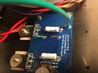
I put a picture below indicating where I measured just to be sure I didn't biff it.
I had to look at the schematic and try to follow the trace, so as is the norm with me, I don't want to waste anyone's time if I did not measure at the correct points. The "Top" of R13, R14, R15 meets R1. I measured at the "Top" of R15 in the pic.I did a continuity check between R8 and R9. The "bottom" of R8 was showing 0 ohm / continuity with the "top" of R9. So, the "Top" of R8 faces the gate resistors according to my overly simplistic look at things. I measured at the "Top" of R8 in the pic.
"Top" is away from the FETs.
R8 is 22.1k. If it matters, R9 is 10k.
I was only able to get to one channel before I was summoned...
I had the R1 pot roughly "centered" and was getting ~503mV. With the pot maxed CW, I got ~421mV. With the pot maxed all the way CCW, I get ~541mV. So, yes. It does change.
Sadly, I have to pause for the evening. If anything come up that you can think of, I'll check in a few hours.
I'll also check the other channel when I get home or in the morning.
This is excellent stuff, and I'm learning as I go. Thank you both!
Attachments
Do what the Mighty Zen Mod suggested; it's just a much simpler way of what
I was asking about.
If things are ok, with your R8 and R9 values and assuming your pot P1 is 5K, you
should see this voltage go from about 6V to 8V as you adjust through P1's range.
It's possible your mosfets have high Vgs, in which case you will need to change R8 to
something higher. But for now, let's just see what the gate voltages are like.
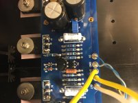
red probe at any gate resistor of IRFP240
black probe at any gate resistor of IRFP9240
fiddle with TL431 pot , write here
Hi ZM -
I did not see your posts earlier. I got called away.
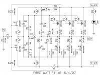
Below is the schematic. It is the one in post #1.
https://i198.photobucket.com/albums/aa276/aeroplane_album/P-F4-1V20-schematic_zps32c28b0a.jpg
Channel 1
Minimum - 3V12
Maximum - 4V01

Channel 2
Minimum - 1V36
Maximum - 1V36

Does not change. Note. Channel 2 is the same channel I measured in post #1485.
As always, with thanks for your help!
Do what the Mighty Zen Mod suggested; it's just a much simpler way of what
I was asking about.
If things are ok, with your R8 and R9 values and assuming your pot P1 is 5K, you
should see this voltage go from about 6V to 8V as you adjust through P1's range.
It's possible your mosfets have high Vgs, in which case you will need to change R8 to
something higher. But for now, let's just see what the gate voltages are like.
Thank you, Dennis! I paused on measuring the other channel until I posted what ZM had requested.
be sure that you have all right resistor values in place , proper orientation of TL431
I'm not familiar with these pcbs , even if Cviller made them eons ago , so can't help with specifics ( jumpers etc?)
if you're sure that everything is OK , replace TL431 (solder good , solder fast) , repeat same measurements and write here
I'm not familiar with these pcbs , even if Cviller made them eons ago , so can't help with specifics ( jumpers etc?)
if you're sure that everything is OK , replace TL431 (solder good , solder fast) , repeat same measurements and write here

be sure that you have all right resistor values in place , proper orientation of TL431
I'm not familiar with these pcbs , even if Cviller made them eons ago , so can't help with specifics ( jumpers etc?)
if you're sure that everything is OK , replace TL431 (solder good , solder fast) , repeat same measurements and write here
Hi ZM -
Is that for both channels or just the channel that does not move with P1? I may have some spare TL431. I'll dig in my stash. Otherwise it'll be several days before I can post results.
Thank you!
Patrick
Hi ZM -
Is that for both channels or just the channel that does not move with P1? I may have some spare TL431. I'll dig in my stash. Otherwise it'll be several days before I can post results.
Thank you!
Patrick
in both channels increase R8 from 22K1 to 27K ; 33K will do also , but , depending of mosfets , you could end with too high Iq in lowest setting ; though , I would use 33K pronto .......
in Mu channel ( undecided one ) replace TL431
report

be sure to start with maxed P1 ; check with ohmmeter , do not trust anyone with rotation directions

Last edited:
- Home
- Amplifiers
- Pass Labs
- A guide to building the Pass F4 amplifier