Does the fragrance influence the art?
Not sure, depends on the artist.
Hi Zen Mod,
Thanks for the tip. I'll head over there and check it out.
Cheers,
Bob
It would be nice to see the LTSPICE sim if you have one handy, I was going
to enter it from your talk.
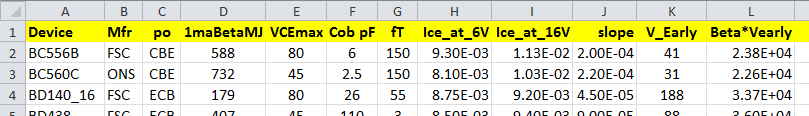
I measured a bunch of PNP transistors and calculated that figure of merit; it's in column "L" of the table below. Beta was measured at (10V & 1mA) and Early voltage was measured at (10V & 8mA). Those were the measurement conditions that most closely met my design needs at the time; readers who don't approve of these choices are, of course, free to repeat the measurements themselves at whatever conditions they prefer.
The KSA992 comes out 11th best (see row 12) in this table. The 2N5401, used throughout Bob's book, winds up in 23rd position, with a Figure Of Merit that's 83% as good as the KSA992. Notice that the top two finishers are large, macho power transistors, and number 3 is the lowly MJE350 medium power device in TO-126 packaging.
It's a big image and the DIYA forum software doesn't display it full-size unless you click on the white cross at bottom left of the image. So, click that please.
_
Nice work Mark, thanks for posting this.
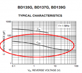
I noticed that you measured most of the values yourself, did you measure the Cob's?
I see the BD140_16 as 26 pF which is much lower than I thought it would be, none of
the data sheet I could find had it listed when I looked several years ago. I think the
very old Phillips data sheet had it but they are not making them anymore and I've read
that the newer parts are not as good - no idea if this is true.
If the current source is being used as the load for a single-ended VAS that is Miller-compensated, bear in mind that the impedance at the VAS output load is really dominated by the low impedance created by the shunt feedback of the Miller compensation. This low impedance persists to quite low frequencies in many designs. The key is that we want very low nonlinearity the impedance of things hangling off the Hi-z VAS node. Also, do not overlook the shunt impedances on this node created by the output stage pre-driver or driver transistors via their Ccb and Early effect, not to mention the amplifier load reflected back through the 2 or 3 emitter followers in a 2EF or 3EF output stage.
Cheers,
Bob
Just to illustrate. This is by no means practical as is. But the idea is to null, cancel, reduce Cob increasing the the impedance BW. The sensitivity is far too high. Change one thing and it's gone.
Attachments
maybe you shoud read Hawksford's paper: https://web.archive.org/web/2013012..._lab/malcolmspubdocs/J10 Enhanced cascode.pdf
and nulling with a linear cap isn't right when we know from the start that Ccb is Voltage Dependent
and nulling with a linear cap isn't right when we know from the start that Ccb is Voltage Dependent
Last edited:
maybe you shoud read Hawksford's paper: https://web.archive.org/web/2013012..._lab/malcolmspubdocs/J10 Enhanced cascode.pdf
and nulling with a linear cap isn't right when we know from the start that Ccb is Voltage Dependent
I did read Hawksford's paper.
The Hawksford's cascode doesn't appear, in spice, to extend the impedance BW. Just the impedance.
I did say this was for illustration not a function model.
an order of magnitude improved impedance at the same corner frequency is still an order of magnitude greater frequency with the same or better impedance for a 1st order slope
and as already pointed out the Z loading the best ccs is still going to be nonlinear, likely more nonlinear with increasing frequency and will typically dominate in aduio power amps
and as already pointed out the Z loading the best ccs is still going to be nonlinear, likely more nonlinear with increasing frequency and will typically dominate in aduio power amps
Something I wanted to ask long ago, what if we throw in a bunch of diodes in series with the output transistors emitter in order to give the driver a little bit more Vce headroom and hence a lower Cob, say 5 diodes for a starter, driver base goes to between the diode string and the resistor, could davada perhaps simulate that for us, thanks.
Something I wanted to ask long ago, what if we throw in a bunch of diodes in series with the output transistors emitter in order to give the driver a little bit more Vce headroom and hence a lower Cob, say 5 diodes for a starter, driver base goes to between the diode string and the resistor, could davada perhaps simulate that for us, thanks.
If we put a series of diodes on the emitter of the output transistor of a 2T current source then we won't be able to bias the the output transistor such that we could get 5mA out of it.
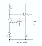
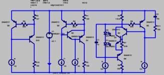
If I understand you correctly your goal is to raise the voltage on the control transistor collector. I think the circuit below will do this and still allow bias of the output transistor.
I think it's the output transistor Cob that is of concern for BW.
Attachments
If we put a series of diodes on the emitter of the output transistor of a 2T current source then we won't be able to bias the the output transistor such that we could get 5mA out of it.
If I understand you correctly your goal is to raise the voltage on the control transistor collector. I think the circuit below will do this and still allow bias of the output transistor.
I think it's the output transistor Cob that is of concern for BW.
Actually I meant, keeping R1 in place and adding the diode string in between R1 and Q1 emitter, but the zener will do the same forcing Q2 Vce stretch a bit as well.
I wasn't so much hoping for a greater BW around Q1, rather was more curious how the driver Q2 interaction with Q1 would change as Cob would almost half with larger Vce, or doesn't the spice model take these changes into account, any way thanks for your effort, maybe there's not much to gain on increased driver Vce.
edit: btw, one could also try decrease Vpwr, which in your simulation looks like to be set at 50 Volt, to something much lower so there's only couple of Volts Vce over Q1, that should also increase Q1's Cob considerably and hence lower the BW, or am I thinking wrong?TOP
Last edited:
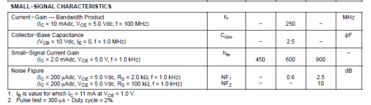
From the ON Semiconductor datasheet
Don't know how I missed that thanks.
Have you considered the BC857S dual PNP that is dirt cheap with 6000 in stock here?
https://www.arrow.com/en/products/bc857s/fairchild-semiconductor
Too bad they are quite small surface mount.
Last edited:
The hFE makes them equivalent to bc857a singles.Don't know how I missed that thanks.
Have you considered the BC857S dual PNP that is dirt cheap with 6000 in stock here?
https://www.arrow.com/en/products/bc857s/fairchild-semiconductor
Too bad they are quite small surface mount.
I think the exact same transistor die is sold in surface mount as "BC857" and is also sold in thru-hole packages as "BC557" see image 1 below.
BC557 is a medium voltage sort bin on a transistor die that can be branded BC556 thru BC560 depending on its measured VCBO and measured Beta at final test. See image 2 below.
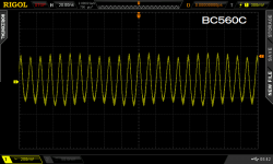
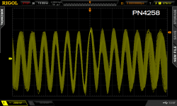
I did test the next higher voltage device (BC556) and the highest Beta device (BC560) see image 3 below. So you can probably interpolate the BC557 / BC857 from these.
_
BC557 is a medium voltage sort bin on a transistor die that can be branded BC556 thru BC560 depending on its measured VCBO and measured Beta at final test. See image 2 below.
I did test the next higher voltage device (BC556) and the highest Beta device (BC560) see image 3 below. So you can probably interpolate the BC557 / BC857 from these.
_
Attachments
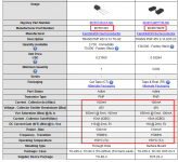
So you can probably interpolate the BC557 / BC857 from these.
_
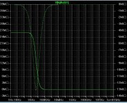
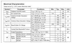
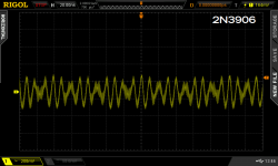
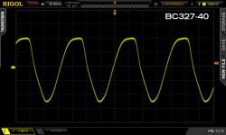
What explains the Cob difference?
What explains the Cob difference?
Mfr=ONS specifies Max Cob
Mfr=FSC specifies Typ Cob
see attachments (hover mouse over image to read Mfr embedded in filename)
Attachments
Hi davada, I would like to purchase your Locky curve tracer if you're not using it any more. (I'd like to have a spare / parts-donor). Would you send me a PM if interested? -- Mark JohnsonThe last time I tried my Locky curve tracer it ate my transistor.
I haven't used it since.
_
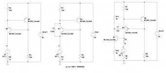
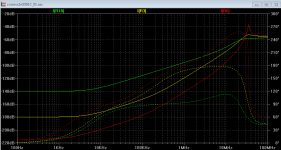
more simmed ccs racing
I think the Cartesian plot used by davada is not very useful, also .AC while convenient is seriously flawed
I used the principles in the Hawksford paper I've been promoting here recently in the following sim, used Cordell models
https://web.archive.org/web/2013012..._lab/malcolmspubdocs/J10 Enhanced cascode.pdf
for me the most informative way of looking at these circuits is the .Tran with a time step small enough to capture the ccs oscillation - too big a t_min and often the sim won't oscillate when it should
then use the actual frequency of interest, show the fft to see nonlinear harmonic behavior:
Attachments
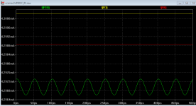
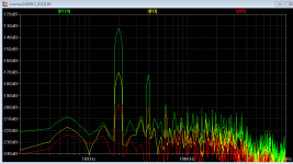
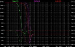
lots of opportunity for unmodeled effects - it would require quite a bit of bench time and good tools to get hardware and sim to match @100 MHz - but I think it is possible - got Fet probes, Vector Impedance Analyzer?
I really was more concerned with showing even audio frequency comparison requires a bit more care with sim, even with the "too simple" models we have in hand
and my characterizing it as "sim racing" should point out how little practical use I think these elaborations have in real world PA circuits where ccs Z and linearity will be swamped by anything they are connected to
Last edited:
- Home
- Amplifiers
- Solid State
- Bob Cordell's Power amplifier book