Finally we have the opportunity to ask ourselves: why does the world's lowest noise device (AD797) use current source loads on the input stage, rather than resistor loads? Are resistor loads STUPID?
Sorry, the guys are right that was very simplified to show the basic signal path. This is more like it. I was simming this with 2N4401/03's and LSK389's a few years ago never made any boards but it was working pretty well.
Attachments

Some people have succeeded in making ultra low noise opamps by using resistor loaded diff amp first stages, and others have succeeded by using current source loaded folded cascode single stage topologies. We have existence proofs that neither approach is impossible. Putting it another way, John Curl devotees are half right: resistor loads are one way, but not the only way, to get a low noise first stage.
Hard to argue with that. Plenty of ways to skin a cat. The conference paper on the 1028 certainly gets into the thermal/current budget and balancing that against the monster input pair.
Bob, I don't understand this - I would have thought that the mirror degeneration resistor might be too high for low noise?
Jan
Jan, take a look at Samuel Groner's critique of D.Self's 5th edition, page 4, Figure 3. Groner built several "model amplifiers" (all TO92 IPS + VAS + classA_EF_OPS) and measured their equivalent input noise with different values of emitter degeneration resistors in the current mirror. What he found in real life, exactly matches what you and I see in LTSPICE ".NOISE" simulations: bigger degeneration resistances in the mirror, give lower noise. Groner realized that measured data on real amplifiers woulld be a LOT more convincing than simulations or equations, and that's what he did.
This forced Self to add a couple of paragraphs to the 6th edition, not quite admitting that he made a design error, but instead marvelling over this discovery of a new noise source (6th edition p.152).
_
Wasn't a Linear Audio short note touching this topic, in your very first volume? I got a copy from the author.
these are all later than the first time I came across this in this Forum.OK, I'll look it up tomorrow at my office.
Jan
I'd guess I read about this here about 6years ago, or more.
True confessions: my 2T current source oscillated!
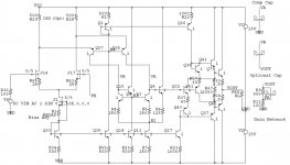
I laid out a PCB of a small power amp a couple weeks ago. It used the 2T current source circuit, seen many places including Bob's book: image #1 below.
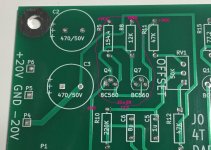
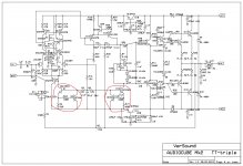
My PCB layout is shown in image #2. It's a dual layer PCB, some connections are on the other side of the board. Schematic (with different reference designators; sorry!) is image #3.
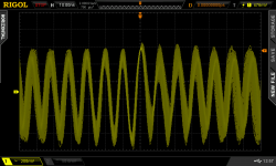
When blank boards arrived, I populated these two transistors, these two resistors, the power supply bypass capacitors, and nothing else. I just wanted to verify that I had correctly calculated the resistance to give (VBE / R) = 4.00 milliamps. And to my surprise, the meter reading was unstable. I connected the oscilloscope and: horrors! Oscillation.
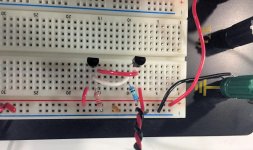
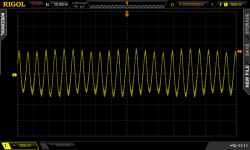
Not believing my eyes, I built up the identical circuit on a solderless breadboard: image #4. Q2 is on the left {its emitter is wired to +VCC} and Q1 is on the right. The white horizontal wire is node EEE and the red horizontal wire is node BBB. Image #5 is a scope photo, the damn thing oscillates even on the protoboard.
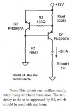
So then I read Walt Jung's article on current sources (here) and found Figure 3A plus accompanying text. D'oh! Image #6.
I laid out a PCB of a small power amp a couple weeks ago. It used the 2T current source circuit, seen many places including Bob's book: image #1 below.
My PCB layout is shown in image #2. It's a dual layer PCB, some connections are on the other side of the board. Schematic (with different reference designators; sorry!) is image #3.
When blank boards arrived, I populated these two transistors, these two resistors, the power supply bypass capacitors, and nothing else. I just wanted to verify that I had correctly calculated the resistance to give (VBE / R) = 4.00 milliamps. And to my surprise, the meter reading was unstable. I connected the oscilloscope and: horrors! Oscillation.
Not believing my eyes, I built up the identical circuit on a solderless breadboard: image #4. Q2 is on the left {its emitter is wired to +VCC} and Q1 is on the right. The white horizontal wire is node EEE and the red horizontal wire is node BBB. Image #5 is a scope photo, the damn thing oscillates even on the protoboard.
So then I read Walt Jung's article on current sources (here) and found Figure 3A plus accompanying text. D'oh! Image #6.
Attachments
I laid out a PCB of a small power amp a couple weeks ago. It used the 2T current source circuit, seen many places including Bob's book: image #1 below.
My PCB layout is shown in image #2. It's a dual layer PCB, some connections are on the other side of the board. Schematic (with different reference designators; sorry!) is image #3.
When blank boards arrived, I populated these two transistors, these two resistors, the power supply bypass capacitors, and nothing else. I just wanted to verify that I had correctly calculated the resistance to give (VBE / R) = 4.00 milliamps. And to my surprise, the meter reading was unstable. I connected the oscilloscope and: horrors! Oscillation.
Not believing my eyes, I built up the identical circuit on a solderless breadboard: image #4. Q2 is on the left {its emitter is wired to +VCC} and Q1 is on the right. The white horizontal wire is node EEE and the red horizontal wire is node BBB. Image #5 is a scope photo, the damn thing oscillates even on the protoboard.
So then I read Walt Jung's article on current sources (here) and found Figure 3A plus accompanying text. D'oh! Image #6.
Because the circuit has both gain and feedback.
You can also compensate the gain with a small, usually 5-10pF, cap in the usual place.
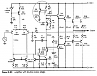
Try to guess why I posted it in this thread, and why I included Figure 3.13 of Bob's book, and why I posted it today, just before the completion of the 2nd edition.Because the circuit has both gain and feedback. ... You can also compensate the gain with a small, usually 5-10pF, cap in the usual place.
I laid out a PCB of a small power amp a couple weeks ago. It used the 2T current source circuit, seen many places including Bob's book: image #1 below.
My PCB layout is shown in image #2. It's a dual layer PCB, some connections are on the other side of the board. Schematic (with different reference designators; sorry!) is image #3.
When blank boards arrived, I populated these two transistors, these two resistors, the power supply bypass capacitors, and nothing else. I just wanted to verify that I had correctly calculated the resistance to give (VBE / R) = 4.00 milliamps. And to my surprise, the meter reading was unstable. I connected the oscilloscope and: horrors! Oscillation.
Not believing my eyes, I built up the identical circuit on a solderless breadboard: image #4. Q2 is on the left {its emitter is wired to +VCC} and Q1 is on the right. The white horizontal wire is node EEE and the red horizontal wire is node BBB. Image #5 is a scope photo, the damn thing oscillates even on the protoboard.
So then I read Walt Jung's article on current sources (here) and found Figure 3A plus accompanying text. D'oh! Image #6.
Hi Mark,
Although I have not had trouble with this current source, I'll look more closely into it and make note of it in my second edition. It is not uncommon for circuits with as few as 2 high-speed transistors in a tight feedback path to raise concerns like this. The current mirror with helper transistor also has this kind of a feedback loop. A cascoded 2EF VAS with Miller compensation has 3 transistors in the loop and also can exhibit some HF stability issues.
BTW, I have also seen the resistor in series with the base in the CE VAS arrangement where that transistor comes into play when current-limiting the VAS.
Thanks for this feedback.
Cheers,
Bob
It is not uncommon for circuits with as few as 2 high-speed transistors in a tight feedback path to raise concerns like this.
The Rush cascode, mother of all oscillation if not carefully damped and layed out.
Thanks Bob.
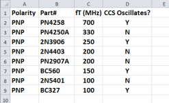
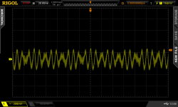
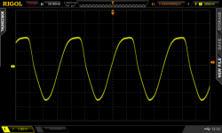
One of the nice things about a protoboard is, you can swap devices easily. So I tried seven other transistor types in addition to the BC550s shown in post #7525. Some of them oscillated in the 2T CCS without base stoppers, and others did not oscillate. I don't see a strong correlation to datasheet "transition frequency" fT but maybe that's not the right datum to study. Here's what I found; hover your mouse over the scope photos to read the part# embedded in the filename.
_
Attachments
Thanks Bob.
One of the nice things about a protoboard is, you can swap devices easily. So I tried seven other transistor types in addition to the BC550s shown in post #7525. Some of them oscillated in the 2T CCS without base stoppers, and others did not oscillate. I don't see a strong correlation to datasheet "transition frequency" fT but maybe that's not the right datum to study. Here's what I found; hover your mouse over the scope photos to read the part# embedded in the filename.
_
Nice work, Mark.
One factor that may influence the tendency to oscillate is the relationship of the current supplied to the "refrerence" transistor to the operating current of the actual current source transistor. The latter is generally chosen to be larger than the former, often by a factor or 10 or so.
The collector-base capacitances of the two transistors may also influence the tendency to oscillate.
One thing I always do is to try to minimize the possibility of my probing the circuit causing it to oscillate due to probe effects like added capacitance. I'll often use a probe with a 1k resistor at the tip, or use a low-capacitance 10:1 scope probe.
Cheers,
Bob
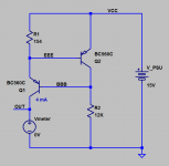
In every case the current source transistor is running at (VBE / 154R) = 4 mA
and the "reference" transistor is running at (15V - 2VBE) / 12K = 1.1 mA
I probed the circuit using Rigol RP3300A probes (image below) connected to a Rigol DS2302A oscilloscope (-3dB bandwidth = 300 MHz).
and the "reference" transistor is running at (15V - 2VBE) / 12K = 1.1 mA
I probed the circuit using Rigol RP3300A probes (image below) connected to a Rigol DS2302A oscilloscope (-3dB bandwidth = 300 MHz).
Attachments

@Bob
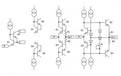
Have you ever seen this used anywhere? On the far left is Barry Blesser's "super" transistor IMO a different take on the CFP, published in 1968 IIRC. I took it in progression to the far right, something that behaves a lot like the two CFP output stage kind of an error corrected (with feedback) buffer. You synthesize a high input impedance from what is inherently a low one rather than a low output impedance from what is inherently a high one, an interesting flip-flop. The designer has a lot more control of the drive end than the load that gets hanged on the output, food for thought.
Have you ever seen this used anywhere? On the far left is Barry Blesser's "super" transistor IMO a different take on the CFP, published in 1968 IIRC. I took it in progression to the far right, something that behaves a lot like the two CFP output stage kind of an error corrected (with feedback) buffer. You synthesize a high input impedance from what is inherently a low one rather than a low output impedance from what is inherently a high one, an interesting flip-flop. The designer has a lot more control of the drive end than the load that gets hanged on the output, food for thought.
Attachments
Last edited:
The Rush cascode, mother of all oscillation if not carefully damped and layed out.
Hi Waly,
Good point about the Rush cascode. A 100-ohm degeneration resistor between the PNP and NPN emitters can help the stability issue in some applications.
Cheers,
Bob
In every case the current source transistor is running at (VBE / 154R) = 4 mA
and the "reference" transistor is running at (15V - 2VBE) / 12K = 1.1 mA
I probed the circuit using Rigol RP3300A probes (image below) connected to a Rigol DS2302A oscilloscope (-3dB bandwidth = 300 MHz).
Hi Mark,
You might try running the reference transistor at 0.4 mA or less and see if the tendency to oscillate falls. Also, it looks like from your diagram that the current output is being connected to the rail through only 1 ohm. Try a 1k resistor, since in most applications the load for this current source will be of moderate to high impedance. The Miller effect introduced by load impedance and Ccb of the current source transistor may be in play in the stability behavior.
Nevertheless, that little 100 ohm resistor in series with the base of the reference transistor is a very inexpensive belt-and-suspenders technique, and I don't think it introduces any disadvantages.
Cheers,
Bob
@Bob
Have you ever seen this used anywhere? On the far left is Barry Blesser's "super" transistor IMO a different take on the CFP, published in 1968 IIRC. I took it in progression to the far right, something that behaves a lot like the two CFP output stage kind of an error corrected (with feedback) buffer. You synthesize a high input impedance from what is inherently a low one rather than a low output impedance from what is inherently a high one, an interesting flip-flop. The designer has a lot more control of the drive end than the load that gets hanged on the output, food for thought.
Hi Scott,
No, I don't think I've seen this circuit. I really like the progression you showed. It would be a fun circuit to SPICE. How is the stability of the right-hand version?
Cheers,
Bob
Nope, once bitten twice shy. YOU can try those mods if you feel inspired. Me, I've switched to low-dropout cascode current sources. That's why I went on an exhaustive search for high Early voltage and low quasi-saturation PNPs: link. The low-parts-count advantage of the 2T+2R shunt feedback current source starts to dissipate, once you begin adding base stoppers and dozen-picofarad compensation caps. Might as well cascode.
Although we certainly DID use the shunt-shunt current reference idea when building Programmable Logic Arrays in all-enhancement CMOS microprocessors. It's an easy way to make the PMOS pullup current exactly track the NMOS process parameters and exactly track the supply voltage. So you get a dependable ratioed low-level ("V_OL") over process, voltage, and temperature variation "corners". But in audio we don't have those problems or those constraints, thank goodness.
Although we certainly DID use the shunt-shunt current reference idea when building Programmable Logic Arrays in all-enhancement CMOS microprocessors. It's an easy way to make the PMOS pullup current exactly track the NMOS process parameters and exactly track the supply voltage. So you get a dependable ratioed low-level ("V_OL") over process, voltage, and temperature variation "corners". But in audio we don't have those problems or those constraints, thank goodness.
Hi Scott,
No, I don't think I've seen this circuit. I really like the progression you showed. It would be a fun circuit to SPICE. How is the stability of the right-hand version?
Cheers,
Bob
It all needs to be explored, the basic circuit with some real models seems fine. Hanged/hung catching up on too many Sergio Leone movies this week.
")
Last edited:
@Bob
Have you ever seen this used anywhere? On the far left is Barry Blesser's "super" transistor IMO a different take on the CFP, published in 1968 IIRC. I took it in progression to the far right, something that behaves a lot like the two CFP output stage kind of an error corrected (with feedback) buffer. You synthesize a high input impedance from what is inherently a low one rather than a low output impedance from what is inherently a high one, an interesting flip-flop. The designer has a lot more control of the drive end than the load that gets hanged on the output, food for thought.
Aren't the right side Q1 and Q3, together with the base diodes, actually current mirrors? If the BE junctions ratio is 1 then the diodes and Q1/Q3 currents are equal and the delta between the base and the collector current sources forward biases the output pair through the 2 diodes in series. Is this some sort of sliding bias scheme?
- Home
- Amplifiers
- Solid State
- Bob Cordell's Power amplifier book