I am simply saying that what difference there is for me, is in the fact that parallel (Schade) feedback still leaves one with an intrinsic pentode, whereas UL leaves one with mainly triode characteristics - through whatever kind of feedback influence.
Is that true? Certainly the source impedance presented to the primary is reduced by the feedback factor. With a low effective plate resistance, I would think that the curves would be more triode-like, and maybe even resemble UL...?
Guys,
I think I may have posted these links on a previous discussion.
From Fritz Langford-Smith on Ultralinear.
http://greygum.net/files/radiotronics/UL.pdf
Parts 1, 2 and 3 all in one file.
A better scan of some of this can be found here:
http://www.pearl-hifi.com/06_Lit_Archive/02_PEARL_Arch/Vol_01/Sec_2/0070_Ultra-linear_Amps_Pt1.pdf
http://www.pearl-hifi.com/06_Lit_Archive/02_PEARL_Arch/Vol_01/Sec_2/0075_Ultra-linear_Amps_Pt2.pdf
In these articles he addresses the 43% tapping suits all tubes myth.
He also states
"These points all indicate that UL Operation is distinctly different from either triode or pentode mode operation and should be regarded as a separate phenomenon"
and-
I haven't re-read these articles recently but I seem to recall that he stated that UL Operation "observed" performance could not be adequately explained by feedback theory alone.
Ians own observations:
The one thing that people tend to ignore (maybe with good reason but maybe not) is that with UL the screen currents will contribute to the output.
One more "shotgun blast at the barn door" - UL feedback to the screens will NOT be as time accurate as a Schade Feedback connection due to the reactive nature of the output transformer.
Cheers,
Ian
Last edited:
"I am simply saying that what difference there is for me, is in the fact that parallel (Schade) feedback still leaves one with an intrinsic pentode, whereas UL leaves one with mainly triode characteristics - through whatever kind of feedback influence."
"Is that true?"
I can see where there would be some difference. In the pentode the forward gm is approx. 3/2 power (really more like 2 power for power tubes), while the neg. Schade feedback is linear. So the inherent forward distortion will take large amounts of Schade feedback to correct down to neglible levels.
In the triode on the other hand, the internal neg. fdbk is the inverse of the 3/2 power, and so in theory could correct the forward error with finite internal neg. feedback (just sets the Mu and Rp). In real tubes though, the g1 is more like 2nd power due to "grid proximity island effect", while the g2 is closer to 3/2 power (until g2 current becomes an issue anyway). So real triodes still distort some.
Possibly one could correct the Schade feedback to near triode mode by putting a thermionic diode from the pentode plate through a resistor to B+, and taking the Schade feedback from the top (plate) of the diode. The current in the diode would track the pentode if the load Z is constant. And the voltage variation on the diode would convert the feedback to the 3/2 power. (ie, when the pentode increases it's gm at increased current, the diode increases the Schade feedback in proportion) Interesting experiment anyway. Probably requires some specific diode conductance to track the pentode and generate enough correction. (ie, both pentode and diode need to be operating over the same exact portion of the 3/2 power curve) Likely have to use some flimsy HV dropping diode like a 2AV2 or something similar.
Or alternately, maybe put some resistance in series with the g2 and tap off the Schade feedback from the g2. (since the g2 intercepts approximately a constant fracton of plate current until plate V gets below the g2 V. This method depends on the load R being constant, to get g2 V to track plate V over the linear range) Might be a good way to prevent the tube from drawing too much g2 current too. Of course this would greatly restrict power output.
Last edited:
One more version of Schade corrector:
Put a high current damper diode in series with the pentode's plate, and take the Schade feedback from the damper's plate. So it's self tracking (diode versus pentode) on the 3/2 power curves this way, but less efficient power wise.
A little inconvenient to float the damper diode that way. So I'm thinking maybe put the damper diode in the pentode's cathode circuit instead. That will lower the pentode's gm, but helps enforce 3/2 power law at g1. The pentodes plate still has the diode correction built in since the output OT is referenced to ground. Would have to simulate this to see how well it works I think. Ehhh... Probably can't get enough diode voltage variation these ways without killing the output power. So likely better to stick with the original diode scheme, merely appended to the plate (an R from diode plate to B+), approach.
Edit:
I think I see the way now. A small thermionic diode from the pentode's grid to AC ground through a resistor. So: Diode's plate to the pentode grid, diode cathode to resistor, then that to - bias V. Then the Schade feedback R goes from pentode plate to the cathode of the diode, probably with a series cap to preserve the bias V. Now as the pentode turns on, the Schade feedback makes the diode conduct more (through the previous driver stage plate R) giving tracking 3/2 power feedback. Easy to configure, and efficient. Have to try this out. Will need something like a HV 2AV2 diode to get enough voltage swing correction on the pentode grid I think.
Last edited:
..... by this time it would have been far more convenient to just use a screen tap on the OPT ")
SY:
I am carefully considering. Look at it the other way round: Take an OPT where the pentode source resistance rp (without feedback) is low compared to the load (an almighty big OPT with a high load, suitable impedance ratio, or simply a constant current load). In a manner-of-speaking, the pentode will still present a set of pentode plate characteristics, not similar to that of a triode. Or if I use a very low load resistor for a triode (say 1 K for a 12AX7) - does the characteristics begin to look like a pentode's - I mean distortion-wise?
(And to those wondering: How does this matter if the driving impedance is lowered? I am thinking of the intrinsic pentode pattern of distortion, with more high-order products than those of a triode. Sure, one is diminishing those by a feedback factor - but so can one with a UL topology. Does that change their ratio to something less prone to listener fatigue? But as said I have to go think ... I have never looked at a constant current loaded pentode with a spectrum analyser. Maybe sit down with Spice before I go on ....)
Guys,
One more "shotgun blast at the barn door" - UL feedback to the screens will NOT be as time accurate as a Schade Feedback connection due to the reactive nature of the output transformer.
... and I need to be careful that I am not standing at the other side of that barn door!
But, inasmuch as an output transformer is reactive (or better, its reactiveness plays a role in the audio pass-band), the plate will then also 'suffer' from the resulting phase angle, thus making the Schade feedback also prone to said reactiveness? (This simply means that the OPT design should be such that its reactive characteristics are negligible or at least small within the audio pass-band. This will naturally have to include leakage reactance regarding the screen taps - which is hopefully achieved in the better types of OPT. Aware of this I have looked at phase angles of screen taps relative to anodes, and have mercifully not found anything of sufficient magnitude to worry me.)
It gets worse when using the cathode feedback type of UL, as e.g. in the classic Quad II. Here the 'common' part of the OPT 'sees' a cathode follower action, i.e. working into a low load. Now one does have to worry about phase performance; this OPT design is a little more difficult - but I digress.
Hello Everyone,
I am resurrecting this thread from the past. After building these amps, they have been performing with no problems for the last 5 years. I am about to start another audio project - some active speakers. To make the equalisation of the speakers easier, it will help if the amps I am using have similar gain. This 6L6 amp with the two stage diff amp at the front has quite a bit of gain. Looking through my posts, it was 12 volts output for 204 mV input, a gain of about 59. I think gain for most commercial amps is about 20. Regardless, I can measure and work out exactly the gain on the two amps.
My question, to get the gain in check, I can either put a voltage divider at the signal input of the amp, or I could try to implement some global negative feedback. If I were to try feedback, where would I inject the signal? I am a little confused with this as the DC offsetg circuit at the grid of the second triode in the first stage adds to the complexity.
Here is the final amp schematic:

Attachments
you may also want to consider output plate to grid feedback....
http://www.diyaudio.com/forums/tube...etter-than-dht-performance-cheaper-tubes.html http://www.diyaudio.com/forums/tubes-valves/177680-schade-feedback.html
http://www.diyaudio.com/forums/tube...etter-than-dht-performance-cheaper-tubes.html http://www.diyaudio.com/forums/tubes-valves/177680-schade-feedback.html
In order to avoid upsetting the DC offset control, if you were willing to add an opamp input buffer you could bring feedback to the input grid via a 20K resistor (very likely along with a phase compensation network). The opamp would simply be a buffer to drive the resulting 1K input impedance, which a humble NE5532 will likely do just fine with very low distortion. Obviously not the purist approach but is probably the easiest way without upsetting your DC control which I imagine is quite helpful as the stages are DC coupled.
Somewhat perversely you could probably, with care and appropriate shielding, implement the whole thing external to the amp in a small box and avoid touching the amp altogether (apart from making sure the amp is inverting, though with opamp trickery you could even avoid that if you wanted), but you'd need a scope to debug it and tweak the phase shift network.
Somewhat perversely you could probably, with care and appropriate shielding, implement the whole thing external to the amp in a small box and avoid touching the amp altogether (apart from making sure the amp is inverting, though with opamp trickery you could even avoid that if you wanted), but you'd need a scope to debug it and tweak the phase shift network.
Last edited:
There are two simple ways to implement feedback and reduce the gain on this design.
GNFB from the OPT secondary can be applied to the grid of the second triode in the first stage.
Lift the grounded end of C14 and insert a small resistor ( 100 to 500 ohms) in series. One end of the resistor to C14, and the other end to ground.
Connect the GNFB resistor from the hot end of the OPT secondary to the junction of C14 and the new resistor. Start with a high value resistor (5K or so) and verify that it actually reduces the gain. You may have to swap the primary OR secondary leads on the OPT to get the phasing right.
Once you are sure that the feedback is indeed negative (reduces the gain) you can reduce the resistor value until the desired gain is reached. Most amps implement a compensation capacitor across the GNFB resistor. This compensates for the peaking in the OPT caused by leakage inductance. It is usually a in the 100 to 1000 pF range and the value is determined by observing the square wave response on a scope. The optimum value is OPT dependent, and your good OPT's shouldn't need a large cap. If you don't have a scope, try several caps in the 100 to 470 pF range and tune for smoothest treble.
As AJT pointed out, "Schade" feedback can be used. It was actually "invented" by an RCA engineer named Schade specifically for making the 6L6 sound more like a triode. It is supposed to only be used with pentode drivers, but small amounts work well with triodes in LTP because of the higher plate resistance in LTP configuration. In this design you would use a resistor from the plate of each output tube to the plate of the corresponding driver. Plate of U3 to plate of U5 and plate of U4 to plate of U6. The resistors should be of equal value, somewhere from 470K to 2 MEG or more, and must be rated for the entire plate voltage swing of both tubes. In this design that would be around 1KV. Resistors with this voltage rating are hard to find, so I use 2 or 3 equal valued 1 watt resistors in series. Say, three 330K resistors in series for 990K. This will increase the plate current through the driver tube by around 1 mA per side, causing the plate voltage to rise a bit. You can increase the value of the plate load resistors to compensate (R11 and R13) or simply bump up the current in the CCS on the cathode to bring the plate voltage back to 295V.
I'm not sure that enough Schade feedback can be applied to achieve the needed gain reduction (about 7 db) in this design, without compromising stability, so some combination, or GNFB only may be the best choice. That depends on your personal preferences, your musical tastes, and how much you want to "mess with success."
A lot has happened since this thread was started. My engineering career of 41 years came to an end, the facility has been sold and is shutting down. I had to move all of my stuff, plus Tubelab twice in the past two years. The first move was on rather short notice, and covered 1200 miles, so a lot of stuff was sold, given away, or trashed. I have recently moved into the house where I plan to be for the next 20 years, but it will be a while before a new lab is finished. I started with an empty 2000 square foot basement, so I have a long way to go.
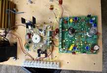
While I was in the temporary housing, I laid out a PC board for the driver section of this amp. I also rebuilt the old breadboard I used for designing this amp.
The 5 year old design is solid, and the only changes were to replace the LED's in the offset adjustment circuit with TI voltage reference IC's, and I changed to 9 pin tubes (6CG7's) to make the board smaller. I got a batch of boards made and they should be available from the Tubelab web site sometime next year. I plan to build a few amp designs with these boards and document everything first, but I need a workbench for all that.
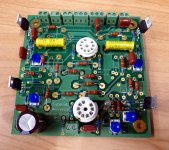
Here is a picture of the board, and my new breadboard. One of the output boards is missing because I blew it up trying to squeeze too many watts through too small a tube! It was a TV sweep tube experiment.
GNFB from the OPT secondary can be applied to the grid of the second triode in the first stage.
Lift the grounded end of C14 and insert a small resistor ( 100 to 500 ohms) in series. One end of the resistor to C14, and the other end to ground.
Connect the GNFB resistor from the hot end of the OPT secondary to the junction of C14 and the new resistor. Start with a high value resistor (5K or so) and verify that it actually reduces the gain. You may have to swap the primary OR secondary leads on the OPT to get the phasing right.
Once you are sure that the feedback is indeed negative (reduces the gain) you can reduce the resistor value until the desired gain is reached. Most amps implement a compensation capacitor across the GNFB resistor. This compensates for the peaking in the OPT caused by leakage inductance. It is usually a in the 100 to 1000 pF range and the value is determined by observing the square wave response on a scope. The optimum value is OPT dependent, and your good OPT's shouldn't need a large cap. If you don't have a scope, try several caps in the 100 to 470 pF range and tune for smoothest treble.
As AJT pointed out, "Schade" feedback can be used. It was actually "invented" by an RCA engineer named Schade specifically for making the 6L6 sound more like a triode. It is supposed to only be used with pentode drivers, but small amounts work well with triodes in LTP because of the higher plate resistance in LTP configuration. In this design you would use a resistor from the plate of each output tube to the plate of the corresponding driver. Plate of U3 to plate of U5 and plate of U4 to plate of U6. The resistors should be of equal value, somewhere from 470K to 2 MEG or more, and must be rated for the entire plate voltage swing of both tubes. In this design that would be around 1KV. Resistors with this voltage rating are hard to find, so I use 2 or 3 equal valued 1 watt resistors in series. Say, three 330K resistors in series for 990K. This will increase the plate current through the driver tube by around 1 mA per side, causing the plate voltage to rise a bit. You can increase the value of the plate load resistors to compensate (R11 and R13) or simply bump up the current in the CCS on the cathode to bring the plate voltage back to 295V.
I'm not sure that enough Schade feedback can be applied to achieve the needed gain reduction (about 7 db) in this design, without compromising stability, so some combination, or GNFB only may be the best choice. That depends on your personal preferences, your musical tastes, and how much you want to "mess with success."
A lot has happened since this thread was started. My engineering career of 41 years came to an end, the facility has been sold and is shutting down. I had to move all of my stuff, plus Tubelab twice in the past two years. The first move was on rather short notice, and covered 1200 miles, so a lot of stuff was sold, given away, or trashed. I have recently moved into the house where I plan to be for the next 20 years, but it will be a while before a new lab is finished. I started with an empty 2000 square foot basement, so I have a long way to go.
While I was in the temporary housing, I laid out a PC board for the driver section of this amp. I also rebuilt the old breadboard I used for designing this amp.
The 5 year old design is solid, and the only changes were to replace the LED's in the offset adjustment circuit with TI voltage reference IC's, and I changed to 9 pin tubes (6CG7's) to make the board smaller. I got a batch of boards made and they should be available from the Tubelab web site sometime next year. I plan to build a few amp designs with these boards and document everything first, but I need a workbench for all that.
Here is a picture of the board, and my new breadboard. One of the output boards is missing because I blew it up trying to squeeze too many watts through too small a tube! It was a TV sweep tube experiment.
Attachments
chrish, here is an amp that I built a couple of years ago: Tube Amps with a Twist: A Push-Pull Amplifier with Simple Plate-Grid Voltage Feedback Driven by a P-Channel FET
The most difficult part of modifying your current amp to a similar scheme would be that you would need a more negative rail for the p-channel fets.
The most difficult part of modifying your current amp to a similar scheme would be that you would need a more negative rail for the p-channel fets.
My question, to get the gain in check, I can either put a voltage divider at the signal input of the amp, or I could try to implement some global negative feedback. If I were to try feedback, where would I inject the signal?
Where to inject the signal? At the voltage offset network that is connected to the first stage. In this amp as it is drawn the signal is the difference between the voltage from that network and the amps input. So you have a perfect place for add NFB.
Yes a voltage divider will reduce the gain but the over all effect of a volume control like that is added noise.
Thanks everyone for the great help.
I think I will start with Tubelab's (and ChrisA) advice for global feedback from the transformer secondary to grid of the second triode in the first gain stage.
I am not sure if I thanked you properly George, but your design has proved trouble free and provided five years of enjoyment. I trust that you enjoy your retirement and you get your lab set up and continue experimenting! Life has been busy for me: working full time while completing law school and being admitted as a lawyer, becoming secretary of our professional association (for primary job of being a pilot), restored a motorcycle and have started a Masters of Law. Time to get back into a couple of audio projects. This next project is not an amp, but speakers. Building a set of Linkwitz LXMinis. All active equalisation with DSPs.
Thanks again everyone with the suggestions and help. I will report back with the results - or more likely - more questions
Chris
If one was to apply the feedback to the 2nd 6SN7's grid, I would have thought the best way to do it would be to connect the junction of the 2 dropper LEDs to earth via a 100 ohm resistor instead of the direct connection, and apply the feedback there. Sort of like the bias spreader in a crude transistor amp. One would have to remove C14 and perhaps add some more filtering to the dropper supply, but it would reduce the effect of feedback signal being subject to nonlinearities of the diodes, or LF phase shift via C14. Just thinking out loud really!
I am not sure if I thanked you properly George
Thanks for the complement, but it was a learning experience for all involved, and I will get to finish my amp soon....just not sure which version, 7403 triode maybe, no 307A DHP, no,......
working full time while completing law school and being admitted as a lawyer, becoming secretary of our professional association (for primary job of being a pilot), restored a motorcycle and have started a Masters of Law
I finally got an engineering degree at age 40 after being an engineer for 10 years, and a masters in engineering at age 47, both while working full time and managing a family......yes, it's a lot of work, but worth it. I abandoned my last muscle car restoration when my job (and the fat salary) ended. I did get to do a few "test runs" and a couple of smoky burnouts with 500+ horsepower on tap.
connect the junction of the 2 dropper LEDs to earth via a 100 ohm resistor instead of the direct connection, and apply the feedback there
So the feedback signal now flows THROUGH the LED's? The feedback current should be very low, so it really shouldn't matter, but I try not to send audio through any silicon junction unless I have verified that it does minimal damage. A mosfet follower is about the only case I have used so far, and even then, the mosfet should be chosen carefully.
I have been using my board as I described, and haven't noticed any weirdness, but I suppose the value and setting of the offset pot (R46) could affect things if a low value pot was used. I think I have 250K and ideally is should be set close to mid range, allowing only a few microamps of signal current to reach the LED's.
I think that one could add a resistor from the wiper of R46 to the junction of R17 and C14 for better isolation. A value as high as 1 MEG or more could be used without ill effect. C14 should be chosen so that the corner frequency is well below audio, but high enough to allow for offset adjustment without undue settling time. .1uF and 1 meg is a 10 Hz corner. 1uF makes for noticeable delay when adjusting the pot, but it useable since you don't adjust the pot often. I wouldn't go any bigger, and use a decent, but not outrageous cap.
If the 6SN7's are matched section to section good enough (requiring minimal offset voltage), it could be possible to replace the C14 cap with a resistor. This would reduce the range of the offset pot, but it is a touchy adjustment anyway.....As said, just thinking out loud, I have not actually tried this.
So the feedback signal now flows THROUGH the LED's? The feedback current should be very low, so it really shouldn't matter, but I try not to send audio through any silicon junction unless I have verified that it does minimal damage. A mosfet follower is about the only case I have used so far, and even then, the mosfet should be chosen carefully.
Admittedly it's not ideal, the diodes set alarm bells ringing in my head but of of course a high value pot spending most of its time very near its central position is unlikely to ever cause a problem with the feedback signal clipping against the diodes, as it ought to never be anywhere near either end of its operation. One benefit of the method I proposed is that the feedback loop can work down to DC which may be less likely to cause an LF resonance.
It may be better to actually put the DC balance on the other/input side, couple it to the 6SN7 via a 1meg resistor and feed the audio in via a 100n cap, and have the feedback network truly DC coupled on the other side. It may be more stable at the low end but then again the feedback levels aren't huge so it may not make much difference at all.
Chris (or George),
Couple of questions about the schematic as published (post #627)
1. Seems the anode voltages of both 1st and 2d stage are way off. Quick arithmetic tells me 1st stage Va should be over 160V and 2d stage over 325 with the published circuit values. Example, 2d stage Va= 400 - (18k*4m) = 328V
Is there a misprint somewhere?
2. With the 2d stage cathode some 160+V above ground, what's the purpose of returning the CCS to -105V? Seems like unnecessary extra dissipation for no benefit.
1. Seems the anode voltages of both 1st and 2d stage are way off
I'm sure that these numbers are the values that Chris measured on his board after he adjusted things the way they worked best for him. I have been using the boards shown in the picture in post #630. They are what I came up with after playing with the design for several years. I use 6GC7 / 6FQ7 instead of 6SN7 for space reasons. I usually set the current through the CCS's for optimum distortion at the output levels I need for the project.
If I need a big drive voltage I set the plate voltage in the first stage on the low side (90 to 100V) to get more headroom in the second stage. With the 7591 tubes that Chris used, there is ample room to set the plate voltages anywhere he wanted. In this case I usually find the first stage around 110 to 120 V and the second stage about 2/3 of B+.
2. With the 2d stage cathode some 160+V above ground, what's the purpose of returning the CCS to -105V?
This designed started with a board that I made about 8 years ago that I deemed the Universal Driver Board. It had the option of AC coupling between the two stages to allow the second stage to run with near zero cathode voltage for maximum output swing. This was for screen drive and cathode follower output stage applications. For this application the CCS could be returned to ground, and indeed it is in my latest board.
I have been tinkering around with the breadboard that I made during this thread, making changes in the design for 8 years. For the design to evolve very little in that time, tells me that we got it right.
The latest schematic is here. The resistor around the mosfet gates allow for negative, positive, or centered on zero bias voltages. Use the combination and resistor values that applies to your design. Use R26 and R24 for conventional negative bias.
The resistors connected to the FB1 and FB2 terminals allow for plate to plate feedback. They will be connected to a similar set of resistors on the output board. Multiple series connected resistors are needed due to the voltages present on the plates in big power tube output stages.....over 2KV! If you don't need this, just leave them out.
Attachments
I usually set the current through the CCS's for optimum distortion at the output levels I need for the project.
Thanks George. Have you ever measured the distortion for the driver board open loop? Particularly h3?
I've been playing with this topology (LTP into LTP) myself for some years now. After trying many combinations I've reached some of the same and some different conclusions :
1. I still like the topology but it's not a slam dunk. I've had to work at it very hard to do better (distortion & gain wise) than a Williamson I built and optimized over the years. My goal for this type of driver is <0.1% THD at 35Vp out with a gain of >x200 and h3<-75dB. That's doable but not easily. Open loop of course.
1. I found that for optimum distortion with most tubes of interest, I needed operating points that wouldn't allow DC coupling unless I use a very large B+for the second stage. Or some form of level shifting.
2. I found that distortion, particularly h3, tends to be high for the 2d stage. You can pick at it changing tubes and operating points, but I haven't found a major cure.
3. I found that I get best distortion performance from triode-strapped high gm pentodes.
Thanks for sharing. Great thread, I'll have to find the time to read it all.
wouldn't allow DC coupling unless I use a very large B+for the second stage
Ditto.
If using this topology for say a 6L6 type tube on 400 volts or so, you don't need a bunch of drive. You still need the entire B+ on the second stage.
My sweep tube amps run a B+ in the 600+ volt range, and I still feed all of it to the second stage. Drive requirements are 100 V P-P or more.
I haven't made a distortion measurement on the new board since my new lab is still under construction, and far from done. I have moved twice since leaving Florida.
I still like the topology but it's not a slam dunk.
I like this topology for many amps, particularly those made with typical audio tubes in triode, UL or Pentode. I made a 3 stage version with triode 6550's as the 3rd stage and a big CCS in the tail. It sounded very nice but only made about 20 watts. 300B's or 45's in AB2 push pull sound good too. No feedback used in any of the triode amps, none needed. Some GNFB or plate to plate feedback was used in the pentode amps.
My other driver of choice is a single pair of pentodes in LTP with some silicon based tricks to raise the gain and lower distortion. These sound more dynamic when used with tubes that have huge current carrying capability, like sweep tubes.
goal for this type of driver is <0.1% THD at 35Vp out with a gain of >x200 and h3<-75dB. That's doable but not easily.
I think I was around 0.25% THD measured at the source of the mosfet while driving the grid of a 300B at the edge of clipping. I had to run through a dozen or so 6CG7's and play with the trim pots to get there, but all of my tubes are well used pulls from military spares that were being scrapped.
- Status
- This old topic is closed. If you want to reopen this topic, contact a moderator using the "Report Post" button.
- Home
- Amplifiers
- Tubes / Valves
- 6L6GC AB2 Amp