Hi Indra1,
I does help indeed, let me look into it. Tonight I bought some ferric chloride so time to make some PCBs. So many interesting project but so little time.
BR,
Eric
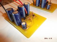
Finally got the right material (laser printer, glossy photo paper and iron) and tonight 2 small PCBs were born
") , results are good for a first time using this method. Thanks Juma for your PCB layout.
, results are good for a first time using this method. Thanks Juma for your PCB layout.Soon I will solder all components and then fire this thing up...
Rgds,
Eric
Hi,
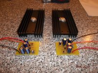
Here are my amplifier module based on Juma's schematic and PCB Layout, I,m only missing an input cap and the output device which will be installed on 1 heatsink per channel.
Each channel has to dissipate 17W for an 8 ohm load for a bias of 0.7A.
My heatsink are recycled and I will if they are big enough install 2 x TO-3 on each of them, but are they big enough ?? By looking at the pics is there a way to find out if they can dissipate 17W with a max temp. rise of lets say 25C ?
They will be installed like on the picture, horizontal. They are 7 inch long, 4 inches wide and the height is 1.5 inch, each heatsink has 8 fins.
To help out I have attached some pictures.
Thanks for your help.
BR,
Eric
Attachments
...s is there a way to find out if they can dissipate 17W with a max temp. rise of lets say 25C ?...
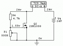
25C temp. rise might be a bit too optimistic for a given wattage on that heatsink, but there is an easy way to check that out.
Mount your MOSFET on the heatsink and make a simple setup (see attachment). Use P1 to set the current (start with lowest resistance of P1) and after you do it wait for about an hour (heatsink needs time to heat up) and measure the temperature of the heatsink, MOSFET and the ambient. Then you'll know for sure.
Attachments
It will make your MOSFETs even hotter. I'll wage an estimate for 17W in horizontal position: 35 C above ambient temp......I will mount them horizontal.....
I'll run some test during the week-end and for fun I'll keep you posted of the dT.
I recently finished a JLH amp where I have to dissipate 36W/ch at idle and my heatsinks were mounted horizontal (identical style) and are OK since I can rest my hand for as long as I want but of course the heatsink where about double the size.
BR,
Eric
I recently finished a JLH amp where I have to dissipate 36W/ch at idle and my heatsinks were mounted horizontal (identical style) and are OK since I can rest my hand for as long as I want but of course the heatsink where about double the size.
BR,
Eric
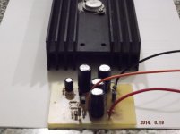
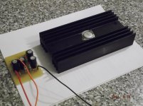
Results are in, Juma you were very close. (5 deg. off only)
For the test, heat dissipated in heatsink was 17W, I needed 2.20V at the gate of the single 2SK134 to get a drain bias current of 0.7A
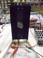
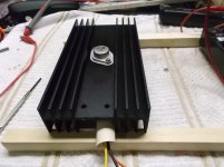
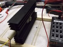
Ambient was 23C, temp reading taken with an Infra-red gun, reading taken after 1h in each of the 3 differents heatsink positions. The coolest is obviously when the heatsink has the fins vertical (standing) but not by so much...I was surprised.
Pic no.1 (left) Vertical position (temp rise of 27C, Heatsink temp 50C)
Pic no.2 (center) Flat (temp rise of 30C, Heatsink temp 53C)
Pic no.3 (right) Horizontal (temp rise of 31C, Heatsink temp 54C)
So to minimize the volume occupied by the amp I'll go with pic no.3
Do you consider 54C as being too hot..?
BR,
Eric
For the test, heat dissipated in heatsink was 17W, I needed 2.20V at the gate of the single 2SK134 to get a drain bias current of 0.7A
Ambient was 23C, temp reading taken with an Infra-red gun, reading taken after 1h in each of the 3 differents heatsink positions. The coolest is obviously when the heatsink has the fins vertical (standing) but not by so much...I was surprised.
Pic no.1 (left) Vertical position (temp rise of 27C, Heatsink temp 50C)
Pic no.2 (center) Flat (temp rise of 30C, Heatsink temp 53C)
Pic no.3 (right) Horizontal (temp rise of 31C, Heatsink temp 54C)
So to minimize the volume occupied by the amp I'll go with pic no.3
Do you consider 54C as being too hot..?
BR,
Eric
Attachments
54C is tolerable but you have to be aware that you measured with both sides of heatsink exposed to free air. When you build the amp one side of the heatsink will be inside the box so you'll have to provide good internal air flow to maintain those figures.
The other thing seems a bit unusual - with all the 2sk135s and 2sk1058s I used that much Vgs (2.2V) gave me Id > 1A. Looks like you have a "lazier" batch of Laterals - nothing wrong with that, just take care to choose appropriate values of collector resistors in the input stage (I'd use 820R for Ic of 2.7mA). Measure the Vgs of your P-channel parts (2sj49) to get the whole picture.
The other thing seems a bit unusual - with all the 2sk135s and 2sk1058s I used that much Vgs (2.2V) gave me Id > 1A. Looks like you have a "lazier" batch of Laterals - nothing wrong with that, just take care to choose appropriate values of collector resistors in the input stage (I'd use 820R for Ic of 2.7mA). Measure the Vgs of your P-channel parts (2sj49) to get the whole picture.
Thanks Juma, excellent point.
p.s. On post 30 you have via a simulation a Vgs of 2.14V for the 2SK1058 (not far from 2.2V that I got)
For my test, my Drain voltage was 24Vdc. In the amp the Drain voltage is really 1/2 supply therefore 12V. I wonder if the value of the Drain voltage (ex 24V instead of 12V) has any effect on the required Vgs for a given Id of 0.7A lets say ?
Can't wait to hear your design ;-)
BR,
Eric
Last edited:
...On post 30 you have via a simulation a Vgs of 2.14V for the 2SK1058 (not far from 2.2V that I got)...
If you read the text in that post and the context that provoked it you'll see that it was an exercise in "simulation can show whatever you want it to show". Models I used there were purposefully flawed in order to demonstrate the point.
I thought it was obvious - my bad...
Well, after some digging I found a way to test both type of lateral MOSFET. With a 24Vdc supply, I adjusted the Vgs to get a static Id of 100mA and then wrote down the required Vgs. Most 2SK134 require 0.7V to get Id of 100mA while most of my 2SJ49 require 0.8V to get 100mA.
I have found some matching pair of 2SK134/2SJ49 but I had a much easier time matching a bunch of 2SK176/2SJ56. Most 2SK176/2SJ56 needed a smaller Vgs to get an Id of 100mA.
Would it be OK to use the 176/56 instead of the 134/49 ?? They do not seem to be as popular on the web so I wonder if they sound OK.
This is a cool project, I'm learning a lot and at the end I know it's going to be a great sounding amplifier.
Thanks for any advice.
BR,
Eric
Well, tonight 1 channel was connected and there was no smoke ;-)
Id is 590mA and DC offset is 190mV, I should of used a pot instead of R3, R5. I think I have to increase the value of R3 and R5 to increase my Id, is this correct ?
I have ordered a 24Vdc, 5A power supply since the one I was supposed to use is too big, can I fine tune the DC offset and Id now with any 24Vdc power supply or does it has to be with the one I will use in the final product ? I believe I'll have to wait but I'm seeking for advice.
p.s. I'll give it a listen tomorrow !
Thank you,
Eric
Last edited:
And the coupling cap on the output needs time to charge up through a route that does not include the speaker.
My interpretation of this is that speaker isolation using some form of delay timer is required to give time for the capacitor to charge to approximately half rail voltage
AND
a resistor route available for this charging current to flow without creating a DC pulse on the speaker.
This is important if a very high efficiency driver were the load.
- Home
- Amplifiers
- Pass Labs
- Recommendation for 5-10W amp.