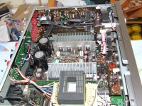
I have concluded that the best engineering solution is to co-locate the filter caps on the same PCB as the amplifier. This way you can keep the tracks short and the radiating area as small as practicable.
Like the problem is solved in Yamaha AX592 integrated amplifier. Test report quote:
... the A-wtd S/N ratio remains some 10dB ahead of the norm at an incredible 93,7dB....
Attachments

Scott, I have often wondered why op-amps with a ground pin are not more common (in fact as far as I know there's only ever been one integrated op-amp that had a ground pin). As an industry insider I would appreciate your opinion on this. Single internally-compensated op-amps with no offset trimming have three "spare" pins in an 8 pin package so I don't really see what the issue is. Having a ground pin means that the relationship between PSRR and CMRR in "traditional" op amps can be broken.
I fear I am never to have an answer to this question, from Scott or anyone else

Bob,
Is the new edition of the book planned to appear soon, or should I buy the first edition?
Hi ivanlukic,
Thanks for asking.
The Second Edition is planned for publication in September of 2014, a little over a year from now.
So I would buy the first edition
Cheers,
Bob
I fear I am never to have an answer to this question, from Scott or anyone else
Hi Harry,
Your question as to why virtually no IC op amps have a ground pin is a good one. My guess would be that there is no sense of need in the industry for that. Maybe the sense is that doing it might not make enough of an improvement to justify it as compared to using the best design practices with conventional op amps (such as making the supplies so clean that they are virtually the same as ground AC-wise). There may also be a concern about the resulting op amp(s) being too odd-ball to have much of a market.
Cheers,
Bob
Say you operated the opamp while modulating the ground pin for whatever purpose. If we operated any power amp this way it's not straightforward to predict all the effects. Therefore designing an opamp with a drivable ground pin will be harder, and it adds another set of fault conditions that must be addressed. I think many designs will not tolerate a moving reference very well.
That is my theory, anyway, based on my understanding.
That is my theory, anyway, based on my understanding.
Hi ivanlukic,
Thanks for asking.
The Second Edition is planned for publication in September of 2014, a little over a year from now.
So I would buy the first edition
Cheers,
Bob
Thank you for that information Bob. I'll wait for the second edition rather than buy the first as it's likely, I hope, to accomodate all of the useful information and criticism in respect of the first edition.
hello,
another reason is that it adds cost which is not justifiable for the majority of the needs.
another reason is adding connections for any pin introduces additional stray capacitance.
It's so good to hear from women in these threads, especially from sorceress. Am I the only one that finds male-only company unbearably boring?
Calling it a VAS is not wrong. In practice it's a voltage change at the input as much as it is a current change that propagates as a voltange change to the output. Using NFB, it's the error signal that drives a stage - you can look at this at either deltaV or deltaI whichever you prefer.
In general I find looking at a common emitter stage as current in voltage out a little bizzare. How about a common source stage with a FET? Now it makes even less sense.
This is a fair way to look at it. Analogously, some prefer to view the amplifying characteristic of a transistor as current gain, while others prefer to view it as transconductance. Some argue over this. Both are "right". If one takes properly into account the various elements of the model and does the math right, the same correct answer comes out. One approach is more intuitive and convenient to some, while that is the case for the other approach for others.
Most terminology is imperfect in its description of whatever, and the choice of which imperfect description to use is not that important. However, it is helpful to be consistent, and that is why I have chosen to adopt the VAS terminology - the same as that used by Doug Self.
Cheers,
Bob
That the second stage of the J. E. Thompson topology is, in fact, a transimpedance stage (TIS) and not a "voltage amplifier stage" ("VAS") is not a matter of opinion or personal preference. This, after all, is Electronic Engineering and not religion.
There are two models of the TIS in existence. The first, and most basic, assumes the second stage transistor of the Thompson circuit is a current controlled current source (CCCS); the second assumes the TIS is a voltage controlled current source (VCCS).
The first order model permits the determination of the location of the dominant pole, the unity gain frequency and amplifier gain at DC and all frequencies preceeding the first non-dominant pole. This model, however, does not accomodate the phenomenon of pole-splitting, but is perfectly adequate for use in the design stage of amplifiers, provided the minor loop is stable.
The second order model, in which the TIS is modeled as a VCCS, is necesarily more accurate and demonstrates the phenomenon of pole-splitting, but is of dubious utility in the design of amplifiers.
Note that with both models the input quantity to the second stage is a current while the ouput quantity is a voltage, even though, with the second order model, current from the first stage develops a voltage across the input of the second stage which drives it.
These facts are summerised in the attached material below which I extracted from an unpublished paper of mine.
Further, here is what Bruno Putzeys has to say in respect of the second stage of a typical amplifier on page 19 of his paper "The F-word" available here:
http://www.linearaudio.nl/linearaudio.nl/images/pdf/Volume_1_BP.pdf
I wonder which "two more famous colleagues" he was referring to here.Under no circumstances should the second stage ever be referred to as the “voltage amplifier stage”. It has a current input and a voltage output. Trying to understand the three-stage amplifier as the cascade of three voltage amplifying stages is impossible and meaningless. I urge my two more famous colleagues to cease this VAS rubbish forthwith. You’re confusing your readers
I look forward to buying what I hope will be a much revised second edition of your book, Bob, given the amount feedback you've received on this forum, provided it contains no incorrect allusions to the non-existent "VAS" in the Thompson topology and its derivatives.
Attachments
Last edited:
It's so good to hear from women in these threads, especially from sorceress. Am I the only one that finds male-only company unbearably boring?
You are not alone.
-RNM
Your question as to why virtually no IC op amps have a ground pin is a good one. My guess would be that there is no sense of need in the industry for that. Maybe the sense is that doing it might not make enough of an improvement to justify it as compared to using the best design practices with conventional op amps (such as making the supplies so clean that they are virtually the same as ground AC-wise). There may also be a concern about the resulting op amp(s) being too odd-ball to have much of a market.
Say you operated the opamp while modulating the ground pin for whatever purpose. If we operated any power amp this way it's not straightforward to predict all the effects. Therefore designing an opamp with a drivable ground pin will be harder, and it adds another set of fault conditions that must be addressed. I think many designs will not tolerate a moving reference very well.
That is my theory, anyway, based on my understanding.
Thanks for the replies. Bob, your thoughts on this are what I expect to be true and kean I hadn't thought of that.
Having said that, both Texas Instruments and Analog Devices have fairly extensive ranges of op-amps aimed at audio applications and I'm a bit surprised that they've never tried to "one-up" the competition. An audio system design needs a good ground system anyway so op-amps that don't make use of it seem to be missing out to me!
I find this talk about a ground reference for opamps curious. An opamp receives it's input as the voltage difference between two nodes, and produces the output signal as the diffierence between two other nodes. Generally (but not always), the input and output have the reference node in common, which is often ground.
The important thing is that the various signal levels remain within the power supply levels for the opamp to work well, best that the power supplies remain stationary with respect to the (common) input and output reference (which can be but not necessarily is ground).
I have no idea why anyone would introduce the complexity to refer something within the opamp to that anyway ambiguous node we call ground.
jan
I find this talk about a ground reference for opamps curious.
Hi Jan,
Some compensation schemes (such as TPC) work better with a ground reference. Essentially it's to do with breaking an inescapable relationship between CMRR, PSRR and open-loop gain that exists if there is no ground reference.
See:
A General Relationship Between Amplifier Parameters, and its Application to PSRR Improvement, IEEE Transactions on Circuits and Systems, Vol. 38, No. 10, October 1991.
Signal reference doesn't need ground. Power supply midpoint doesn't need ground but may need to be referred to the signal reference. That compensation return to 'ground' is really a return to the signal reference, isn't it?
I may have missed that paper you mention - is it available online?
jan
- Home
- Amplifiers
- Solid State
- Bob Cordell's Power amplifier book