The power circuit is working. It is easy to hear the improvement of linear regulator and no DC converter. Cut the trace is working. ") Maybe no need for isolator.
Maybe no need for isolator.
I use 3R 1W for replacement FB1. I use 10.1R 5W for 1V regulator input. 10.1R gets hot @ 40 degrees above room. XMOS is 24 degrees above room. Power is in the attached.
Maybe no need for isolator.I use 3R 1W for replacement FB1. I use 10.1R 5W for 1V regulator input. 10.1R gets hot @ 40 degrees above room. XMOS is 24 degrees above room. Power is in the attached.
Attachments

Here is trace for M1 M2 I cut and turn off Dc converter. I also add 100uF after 3R, and add 10uF ceramic after 10R, and 470uF polymer cap after 1V regulator. It is finished and the sound is very good. XMOS is excellent ! I agree with the review that said XMOS is best.
Attachments

Thank you for many diyer asking about the decoupling cap distance
A photo with a ruler is used for better visual understanding. The current design is 2mm from the chip, if you find your design has decoupling cap longer than 2mm distance is considered to be too long and poorly design
Any suggestion and improvement are always welcome!
An externally hosted image should be here but it was not working when we last tested it.
Hi DIYinHK
Regarding decoupling. A thumb rules is that 1mm pcb path = 1nH. So there may be 2mm from the edge of the Xmos chip to one end of the caps termination. The other end of the cap has approx 1mm to the via and extra 5mm back to the edge of the Xmos chip. But the edge of the Xmos chip is not correct point to measure from. the correct point is the dedicated Vdd pin and the related Gnd pin. this may be 2-5mm extra. A total of 10 to 14mm = 10 to 14nH in serie with the decoupling cap. Placement of the via is also not optimal. The optimum placement of the via is on the side of the caps GND pad and not the end of the caps GND pad. this wat you can keep the PCB distance to the thickness of the PCB + a bit more = 1.5mm+1.5mm(2*PCB thickness)+2mm(heat relief) = 5mm = 5nH. Please also place the via closer to the Caps GND pad instead of using long heat relief between the caps GND pad and the via.
A better way to decouple (read low pcb inductance) is to place the cap on the button side of the PCB, direct under the Vdd and the related GND.
If you dont want to mount components on the button side , then pleace rotate the cap 90dgr so the Caps GND pad places closer to the Xmos chip.
Last edited:
Did you request "QUOTE" for the part number input of;
NZ2520SD-22.579200M-NSA3449C
NZ2520SD-24.576000M-NSA3449C
and did their quote replies after a couple days later say "out of stock"?
You always need to request "QUOTE" and wait for their reply.
Hi.
No I did not quote. because the price for shipping the osc to Denmark is 75USD.
I have instead contacted the local distributor for a "stock" sample around 25Mhz. This may be quicker and for less penny

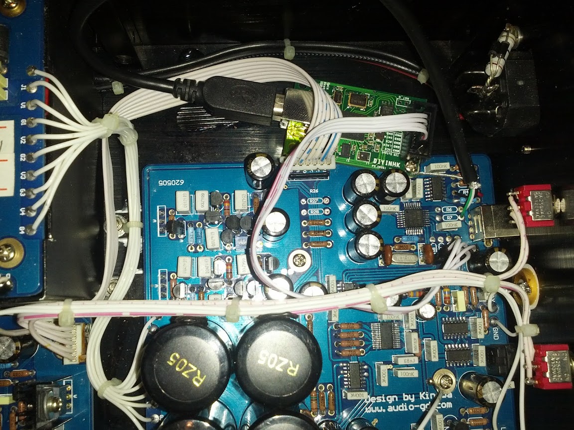
I add isolator TI ISO7640M. I Supaglue extra PCB.
Hi..
Did you decouple the isolator?
If not please try this.
Solder a SMD 100nF between and direct on pins Vcc1-GND1 and Vcc2-GND2.
combine with e-lyt as close to the pins as possible.
Attachments

is this manufacturer training?
it seems the best way forward is to wait for second or third generation boards (1month) after customer feedback. good for modding though and the price is right if thats what you are after.
love the rolling eyes emoticon, nice touch. these are real issues caad brings up (and the very same ones I keep bringing up) that should be taken into account.
it seems the best way forward is to wait for second or third generation boards (1month) after customer feedback. good for modding though and the price is right if thats what you are after.
diyinhk said:Thank you for many diyer asking about the decoupling cap distance
love the rolling eyes emoticon, nice touch. these are real issues caad brings up (and the very same ones I keep bringing up) that should be taken into account.
Last edited:
is this manufacturer training?
No..
But if the little chip (read Isolator) not is proper decoupled it will make influence on the jitter. I did not see proper local decoupling of the isolator on the photo ;-)
Last edited:
Photo is show and tell, not final, but of course it is already decouple with x7r exactly on the pin. It is basic thing.Hi..
Did you decouple the isolator?
I will improve power routing, i2s gnd return, etc etc for final build. I am finished for the modifications so now is time to do final build.
I change resistors on input to iso7640m from 100R thick film to 15R thin film and improve solder. The sharp has gone. It is not the iso make this sound. It is my bad solder and wrong resistor. I use Vishay melf resistor
http://docs-asia.electrocomponents.com/webdocs/0d99/0900766b80d99de8.pdf
I also move iso power wire direction so it is next to ground wire and not across signal line and iso. It is from LP5900 near the xo. Also add 22uF tantalum on iso power input across X7R.
No more to do. So, now the next toy for playing....
A good thing for this XMOS - the driver is very stable. I cannot get dropout - music plays w/o any error continuously, even the PC is changing LAN etc.
Here is final ( I hope ).
And the next project ... is ... ES9023DAC PCM2706 CS8421 192KHZ 24BIT LM4766 Omron USB DAC Kit WLX | eBay
Here is final ( I hope
).And the next project ... is ... ES9023DAC PCM2706 CS8421 192KHZ 24BIT LM4766 Omron USB DAC Kit WLX | eBay
Attachments

I hacked it in my good old Audio-gd Compass. Removed power from PCM2707 (R27, R28), removed 75ohm i2s resistors (R8-R11) and soldered pins there, removed USB input resistors (R6,R7) and soldered a USB cable there (so I can change the module . R4 was 1MOhm resistor between usb Vcc and GND used for PCM2707 powerup on Compass powerup - used that point for power connection to the internal USB cable. Didn't bother going for the internal +5V line across the PCB, used USB power connected only to the XMOS. XMOS is always on when USB is connected and not only when the whole unit is powered on. Works like a charm! No more 16bit 44.1/48 resampling.
. R4 was 1MOhm resistor between usb Vcc and GND used for PCM2707 powerup on Compass powerup - used that point for power connection to the internal USB cable. Didn't bother going for the internal +5V line across the PCB, used USB power connected only to the XMOS. XMOS is always on when USB is connected and not only when the whole unit is powered on. Works like a charm! No more 16bit 44.1/48 resampling.
Last edited:
DIYINHK,
I have the board hooked up to your ess9018 board and I am not getting any sound. The lock light is on.
I know the DAC works since I can run it with the CM6631. I uninstalled the CM drivers and restarted the computer. I tried it with the Windows player and JRiver. I get no errors on playback. The drivers say everything is OK. Any idea what I missed?
John
Problem Solved. Sometimes it is too simple. I assumed that the connections where all good since I had a lock light. Not so. I had a cold solder joint on the LRCK line. I hate those darn things. Now it works great. The mute light did not go on with the bad connection when the lock light was on and the player was paused. Now it works right.
I'm so. Many thanks to every body and diyinhk.
Hope DIYinhk issue the next pcb for more sound quality and DAF(diy's accept factor) .
1) xmos with individual linear regulator( for each +V pins of xmos ,
) and each oscilators , and change the layout for shortest I2S output nearly the xmos or add the buffer/isolator like 74v125 or better.
2) AK 4399 with more srortest output trace ,resistors ,I2s in + add ak4413-15 ob board for take 24/192 via other spdif device.
Done, and just compare to my current usibg dac.... ,The SQ is improved from my current dac(te7022L>I2S>AK4395) .
I like this dac set.
but,The XMOS bord not don yet ,still need to do more modify.
I like this dac set.
but,The XMOS bord not don yet ,still need to do more modify.
Attachments


Last edited:
- Status
- Not open for further replies.
- Home
- Source & Line
- Digital Source
- New XMOS usb 384khz