Ok shipping waived for next 48 hours. Joining us today brings us closer to the 30,000 review mark. Your contribution to the state of the art counts. Creates an opportunity for you to experience an exotic amplifier and share with us your experiences. There is no amplifier out there like this one.
Last edited:
Ok shipping waived for next 48 hours.
An externally hosted image should be here but it was not working when we last tested it.
OnAudio,
thanks for the references. I had already ordered some Elna capacitors of that same value when I order the other parts for the build, I'll assume they are comparable for now. On the small film capacitor so that I am clear on this subject. From what I have read the film capacitors value is not that important right, just that there is a film capacitor in parallel with the electrolytic cap and removes issues with those caps. So if I happen to have a 10 or 100 mfd 100v cap sitting around would it matter if I just used that value or is there a problem with using a higher value cap? On the rectifier side are there any special qualities of one over another. Does the speed of the rectifier have anything of consequence here, would a Schottky diode bridge have any advantage here?
It is recommended to NOT place small film caps in parallel with large electrolytics. See:
http://www.diyaudio.com/forums/power-supplies/106648-paralleling-film-caps-electrolytic-caps.html
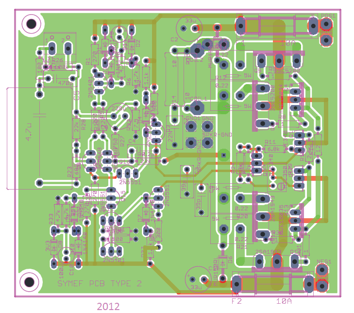
The PCB will look something close to this
Here is a draft of the PCB. This is just a draft the silk will be cleaned up. Show your interest here. Once we get 10 members the PCBs should be ready within 1 week. It will be 2 layer, 3 oz , lead free. A contribution of US $15 per PCB will be appreciated. Kindly show your interest here. You can read reviews for this amplifier here: Gallery
Here is a draft of the PCB. This is just a draft the silk will be cleaned up. Show your interest here. Once we get 10 members the PCBs should be ready within 1 week. It will be 2 layer, 3 oz , lead free. A contribution of US $15 per PCB will be appreciated. Kindly show your interest here. You can read reviews for this amplifier here: Gallery
Attachments
Last edited:
Here is a draft of the PCB. This is just a draft the silk will be cleaned up. Show your interest here. Once we get 10 members the PCBs should be ready within 1 week. It will be 2 layer, 3 oz , lead free. A contribution of US $15 per PCB will be appreciated. Kindly show your interest here. You can read reviews for this amplifier here: Gallery
How do you plan on mounting the output transistors on a heatsink with this configuration? The best thing would be to mount them underneath but you would need to make some holes on the PCB to accommodate this.
Ciao!
Do
I believe that for easy servicing, the power transistors should be mounted flush against the board and heatsink and use the PCB with screw and washer as pressure plate. The other transistors could have a bigger hole to fit a screw through the board.
Doing it your way is not bad but if you have to replace one of the transistors, you basically have to unsolder all of them which could damage the board/components and is time consuming.
Also think of how to properly measure the proper hole distance on the heatsink is going to be a challenge and aligning all the pins at once to put back the board over is going to be challenging as well
Just my 2 cents!
Do
Last edited:
Thanks Pinnocchio. However in the case that an amplifier fries its output stage, in most cases it fries all the output transistors.
I have edited my post above
OnAudio, might I offer a couple of suggestions re. the layout?
1. the schematic shows 33uF caps on either side of the fuses. this is actually quite a nice idea - the fuse is a free L-R network
2. you're paying for a 2-layer PCB, so why are you throwing away almost all of the Cu on one side?
3. have you thought about the symmetry of this layout?
4. have you looked at the high current path for +ve and -ve transients (cap-bjt-spkr-spkr_return-cap). specifically, look at where the return current must flow to get back to the 33uF capacitor. Assume the speaker connections are joined with a straight wire link flush to the pcb - that way you get to ignore the speaker & its interconnects, and can see the PCB contribution alone.
what you will then see is that the return path (your 0V plane) is chopped to pieces - needlessly so. you can fix the worst of it by changing non-0V interconnects to the opposite layer. the next step would be to adjust component spacing and/or pad-pour clearances to remove as many small "slots" as possible (I use placement rules that allow Cu pours to flow between adjacent pads & vias - these Cu pour "slots" are often major sources of EMI, and are usually generated automatically).
you will also see that the trace routing betweeen fuses, 33uF caps, transistors & output is far from optimal. locate the 33uF caps such that all output current must flow past the cap (at present it does not). ideally you would have the 33uF cap placed midway between the two collectors, with the fuse feed there. symmetry is a simple way of equalising impedances. its also the best way, but if you have a solid 0V plane its possible to adjust trace widths to (somewhat) compensate length asymmetries
once you start looking at the layout symmetry, lots of things become apparent. I would place the speaker terminals adjacent, then locate the power transistors and 33uF caps to give the most symmetric power stage layout. and no doubt spend the best part of a week playing with that in conjunction with the heatsinking.....
Thank you Terry. Very much appreciated
, although I am willing to learn
Yes I have looked at at it and exploited it in a way
Although the ground is chopped to pieces it is still potent to some extent, hopefully, maybe you could tell me more. about clearances, I am trying to avoid destructive capacitative coupling as much as possible. Many amplifiers do not even implement a ground pour (The symef pcb type 1 actually only implements a partial ground distribution ). In one of the threads it was even mentioned that the non ground pour Leach amp PCB sounded better. This may be due to misunderstanding how the ground system works. (I stand to be corrected)
OnAudio, might I offer a couple of suggestions re. the layout?
1. the schematic shows 33uF caps on either side of the fuses. this is actually quite a nice idea - the fuse is a free L-R network
Minimizing unwanted parasitic interactions between some traces and ground2. you're paying for a 2-layer PCB, so why are you throwing away almost all of the Cu on one side?
Spent quite some time3. have you thought about the symmetry of this layout?
, although I am willing to learn4. have you looked at the high current path for +ve and -ve transients (cap-bjt-spkr-spkr_return-cap). specifically, look at where the return current must flow to get back to the 33uF capacitor. Assume the speaker connections are joined with a straight wire link flush to the pcb - that way you get to ignore the speaker & its interconnects, and can see the PCB contribution alone.
Yes I have looked at at it and exploited it in a way
what you will then see is that the return path (your 0V plane) is chopped to pieces - needlessly so. you can fix the worst of it by changing non-0V interconnects to the opposite layer. the next step would be to adjust component spacing and/or pad-pour clearances to remove as many small "slots" as possible (I use placement rules that allow Cu pours to flow between adjacent pads & vias - these Cu pour "slots" are often major sources of EMI, and are usually generated automatically).
Although the ground is chopped to pieces it is still potent to some extent, hopefully, maybe you could tell me more. about clearances, I am trying to avoid destructive capacitative coupling as much as possible. Many amplifiers do not even implement a ground pour (The symef pcb type 1 actually only implements a partial ground distribution ). In one of the threads it was even mentioned that the non ground pour Leach amp PCB sounded better. This may be due to misunderstanding how the ground system works. (I stand to be corrected)
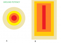
This is desirable but may shift the origin of the ground plane. This may not be a bad thing and provides fast transient response close to where it is needed. I hope that the attached diagram shows how the two capacitors modify the distribution of the ground plane. In this situation it takes on shape B. Placing the origin right where we want it. Also the PCB is only 4*3.5 in dimensionyou will also see that the trace routing betweeen fuses, 33uF caps, transistors & output is far from optimal. locate the 33uF caps such that all output current must flow past the cap (at present it does not). ideally you would have the 33uF cap placed midway between the two collectors, with the fuse feed there. symmetry is a simple way of equalising impedances. its also the best way, but if you have a solid 0V plane its possible to adjust trace widths to (somewhat) compensate length asymmetries
I look forward to a productive discussion. Kindly post your layout ideasonce you start looking at the layout symmetry, lots of things become apparent. I would place the speaker terminals adjacent, then locate the power transistors and 33uF caps to give the most symmetric power stage layout. and no doubt spend the best part of a week playing with that in conjunction with the heatsinking.....
Attachments
OK, starting with stray capacitance. the general guideline is based on i=c*dV/dt. Any nets with high dV/dt are sources of noise, and high impedance nets are receivers. IME stray capacitance between nets is much worse than stray capacitance to 0V.
you can group the various nets into 3 basic categories wrt stray capacitance:
1. beneficial:
some nets (eg supply rail, current source base network) benefit from capacitance to 0V
2a. Meh - if the node voltage doesnt change much (low dV/dt, one of the advantages of steering currents) then its probably not an issue. likewise if the node can sink/source bags of current, such as output stages
2b: compensatable - in many cases the effects of stray capacitance to 0V can be compensated by adjusting component values, eg on the MJE340 base net
3. bad
I dont know much about audio amps, but if I read this schematic correctly, its pretty nice. bags of current steering, and symmetrical topology so good slewing each way, and should inherently cope with quite a bit of stray capacitance to 0V.
its good to identify nodes where C_0V is beneficial - when the layout is done they can be flooded with Cu. and you'll want to identify where C_0V is bad, because in addition to ensuring C_0V is small, those areas will be most sensitive to external electric fields. If you want to minimise susceptibility to these, a good 0V plane is an excellent start (and often suffices).
IOW if you're going to have a problem with stray capacitance to 0V, it'll be in the low power section.
the converse applies for stray inductance. V = L*dI/dt - so loops of rapidly changing current are the sources, and other loops are the receivers. the power stage and the PSU have some pretty decent currents flowing, so these are the sources.
so you want to minimise loops in your power stage to minimise the associated magnetic fields, and C_0V isnt much of a concern. So a good 0V plane and low inductance interconnects are the go here.
and the low power stage wants its loop area minimised as well, minimising current induced by internal (power stage& psu, other channels, xfmr, wiring) or external magnetic fields.
lastly there is the issue of "star-pointing" the low- and high-power sections. what you're really doing here is adding some deliberate "slits" to an otherwise excellent 0V plane (or joining two separate 0V planes together in a controlled manner), to prevent power stage & psu currents from flowing in the low power area (2 pcbs would be a great approach here). the trick is to remember not to run any traces over the slits (unless they are heavily LP-filtered) - in this case you would have 4 traces (V+, V- & the two current drives) on the opposite side of where the two 0V planes are "star-pointed", which probably should be at the speaker return terminal. quite do-able.
HTH
Sorry Harrison,
Dealing with a crashed computer...... DAMNED hard-drive failures.....
Steven
Thanks for the update Kindhornman
. Sorry about your drive.Good news....parts landed from Mouser USA to New zealand in 3 days!!! love those guys!
Bad news....parts delivered to office and I have been on the road all week, will have to wait till Monday now
Thanks for the update Dagwood. Yes that was fast. Dont worry just relax and enjoy your weekend.
Thanks Terry. Everything you have discussed has been considered. But do point out areas that I skipped . This PCB features good overall global optimizations and this may have been achieved by adjusting some local optimization. (Kind of take some from here put it there for a more stable overall performance) I say put yourself down for 2 or more PCBs and lets take this baby on the road
. This PCB features good overall global optimizations and this may have been achieved by adjusting some local optimization. (Kind of take some from here put it there for a more stable overall performance) I say put yourself down for 2 or more PCBs and lets take this baby on the road Harrison,
I measured with a micrometer where I was attempting to install the first resistors. The spacing appears to be 11mm center to center on the hole pattern. The resistors I received from Digikey, your part numbers have a body length exactly the same as the hole distance. I would have to fold the leads straight down and bent in to install in those holes. I am just going to mount them vertically instead and bend one lead over and down unless there is some reason not to do that.I also received a complete set of resistor values I ordered on Ebay that are all 1/4 watt 1% resistors that are much smaller than the ones from DigiKey. I could just substitute these in the place of the ones you called out? I'll wait before I solder anything in place until I hear back from you. I did fix my computer, it was a dead hard-drive, spins up but can't be recognized by the computer or another I tested it on. Luckily it had a 5 year warranty from Seagate and a new one is on the way, but I had to rewrite the MBR to get back in. Luckily the drive only had my Linix install on it and no information was lost. But it was a drag and now I will have to reinstall the Linix when the new drive shows up and again redo the Master Boot Record. What can you do, it is either Western Digital or Seagate, they are all that's left for drives and they both have their detractors, just like 5532 opamps......Now if it had been a SSD drive and my information was on that would I be pissed, no recovery from one of those when they crash. And yes I do back up to an external hard drive, not that stupid. But the cloud no way, not that stupid either.....
I measured with a micrometer where I was attempting to install the first resistors. The spacing appears to be 11mm center to center on the hole pattern. The resistors I received from Digikey, your part numbers have a body length exactly the same as the hole distance. I would have to fold the leads straight down and bent in to install in those holes. I am just going to mount them vertically instead and bend one lead over and down unless there is some reason not to do that.I also received a complete set of resistor values I ordered on Ebay that are all 1/4 watt 1% resistors that are much smaller than the ones from DigiKey. I could just substitute these in the place of the ones you called out? I'll wait before I solder anything in place until I hear back from you. I did fix my computer, it was a dead hard-drive, spins up but can't be recognized by the computer or another I tested it on. Luckily it had a 5 year warranty from Seagate and a new one is on the way, but I had to rewrite the MBR to get back in. Luckily the drive only had my Linix install on it and no information was lost. But it was a drag and now I will have to reinstall the Linix when the new drive shows up and again redo the Master Boot Record. What can you do, it is either Western Digital or Seagate, they are all that's left for drives and they both have their detractors, just like 5532 opamps......Now if it had been a SSD drive and my information was on that would I be pissed, no recovery from one of those when they crash. And yes I do back up to an external hard drive, not that stupid. But the cloud no way, not that stupid either.....
Last edited:
- Status
- This old topic is closed. If you want to reopen this topic, contact a moderator using the "Report Post" button.
- Home
- Vendor's Bazaar
- Combined Onaudio thread. (23 threads)