Eivind, i feel the same way. You can see that in this thread that Nagys stubbornness is partly due to him wanting to stick to the goldmund clone that others have tried to steer him from doing. I see both arguments, Nagys for staying true to his OP and others just trying to help. It has happened more than once where Nagya was off on something but stood his ground since so many other points were trying to get him to change something taking it away from the goldmund schematic. His own way saying he was wrong is like asking for help on grounding issue, lets fix it then move on. It just pesonalities that are obvious nothing more.
Everyone here has there own interset here or they wouldn't be posting. I don't think it is about protecting those that don't know better. Please no more I'm a engineer or the schematic is 100% right comments, it's just stirs the pot and will always bring negative feedback.
This thread has come along way keep up the great work, it's much appreciated.
Brad
Thank you for posting that picture Alex. As far as I'm concerned, this board is finished. It's easy to build and because of the ground plane, gives tons of options for grounding schemes. For those who don't want large currents on the ground plane near the input stage, just solder everything (speaker ground, transformer ground, etc.) on the ground plane all close to each other at the bottom of the board. Just bellow the 60VAC input. Done and done.
Its a pity that those who have criticized the grounding and have pointed out alternatives don’t see any reason to contribute any longer about that question.
well, I suggested the best place to connect speaker minus/ground, right where supply ground is connected to board
in a direct comparison you may hear only a very small difference, and maybe even close to imaginary
so it might not matter that much
maybe all that makes a difference is a few solder joints more, or less
as it is now, you can try both
")
but I think there have been a lot of confusion about small matters like component polarity, orientation, etc
even the function of plated through holes seemed a new thing, and obviously caused some confusion about how to solder
small matters, but still enough to give the feeling of uncertainty
from that perspecive its not right to say that a few critical members caused any confusion
on the contrary
that ongoing debate gave the time to correct errors
and there have been lots of corrections
even after it was announced to be ready and done
I cant count the number of times it has been ready to go
and there could still be some small silly mistake
until its been tested in real life, its a kind of gambling
if you want the boards, fine
personally, I actually do have a small collection of various boards too
but as suggested early on, please wait with buying all the parts, and mounting, until its been tested
Attachments
Yes, the ground plane gives many options. Different builders can solder their ground points to different places on the board. If you want to keep high current away from the input stage, solder everything on the bottom of the board next to the power supply. This is all the more important not to have a solder mask. It makes it significantly easier to try a few different options while building.
Bigpanda - I think it's safe to proceed with the group buy. What are your thoughts?
Everyone else who would like to participate in the group buy for the boards, please go here, read post #6, and contact Bigpanda: http://www.diyaudio.com/forums/group-buys/175296-pcb-order-goldmun-clone.html
The boards will come in pairs (you'll need 2 boards to build a stereo amplifier). The boards will be tin plated and have nice thick copper traces.
Alex, I have one more request for you, hopefully this will be the last change Can you please switch the positions of C33 with C32 and also C36 with C35? The smaller capacitors (1uF) should be closer to the MOSFETS. This can affect the sonic quality of the amplifier. Thank you.
Can you please switch the positions of C33 with C32 and also C36 with C35? The smaller capacitors (1uF) should be closer to the MOSFETS. This can affect the sonic quality of the amplifier. Thank you.An update for the GB has been post on the GB link. Buyers pls read it over there.
http://www.diyaudio.com/forums/group-buys/175296-pcb-order-goldmun-clone-10.html#post2347111
http://www.diyaudio.com/forums/group-buys/175296-pcb-order-goldmun-clone-10.html#post2347111
T6 is connected correctly, we've been over this a million times. Goldmund connects it backwards for their reasons that ONLY they know why If anyone wants to build it with the C-B shorted instead of E-B, all one has to do is rotate the transistor 180 degrees and solder it in backwards on the PCB. No big deal. The amp will function both ways, although it might be more stable if connected the original Goldmund way, because again, they have their reasons for doing so.
If anyone wants to build it with the C-B shorted instead of E-B, all one has to do is rotate the transistor 180 degrees and solder it in backwards on the PCB. No big deal. The amp will function both ways, although it might be more stable if connected the original Goldmund way, because again, they have their reasons for doing so.BV - I cannot argue with you, because you're correct. That's how it usually is supposed to be connected. The very latest unpotted Goldmund modules (essentially A2 modules) use the new MPSA42 transistors, where they short C-B and bypass the Zener diode with a 1u capacitor.
However, the old Mimesis series of amps (with A1 modules), used BC182B transistors and shorted E-B. They also had no bypass capacitor for the Zener diode. The old Mimesis amplifiers had a very magical sound and that is what this entire thread is about. Cloning the old Goldmund Mimesis 9.2, Mimesis 3, and Mimesis 6 amplifiers. The PCB should follow the old design/schematic. As it stands, T6 is connected correctly. If any potential builders want to use an A2 module's configuration, it's up to them to make the necessary modifications on the PCB. If anyone wants to use the A2 module, here are the changes you'll need to make, READ CAREFULLY!!:
1.) Replace T3, T4, T5, and T6 with MPSA42 transistors.
2.) On T6, short C-B instead of E-B.
3.) Bypass the 6V Zener diode with a 1u film capacitor.
4.) Replace R11 (20K) resistor with a 10K resistor.
5.) Change the BIAS resistor R23 (330R) by soldering in parallel a 1K to 1K5 resistor. Goldmund's service manual gives a range here, so if the MOSFETS are still overheating, you'll have to go with the lower 1K resistor value.
This info is directly from Goldmund's service manual. After the changes, the amplifier should perform 100% correctly.
Now everyone can stop crying about the T6 transistor and use an A2 module where C-B is shorted.
Attachments
Last edited:
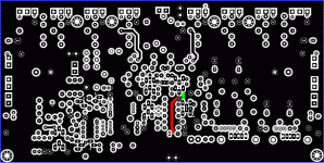
The devil's in the details...
The PCB's not laid out the way I would have done it, but it does have one very nice feature:
There's a wide copper track (shown in red below) connecting the input ground to the ground of the feedback network, providing a nice low-impedance path between those two points. It's also almost completely surrounded by holes in the earth plane, so very little of the high current muck will find it's way to and through that track. This means very little hum and distortion will be injected into the input stage.
Isolation could be further improved by adding another little cut in the ground plane as shown in green below.
edit: OK, do I get shot now for finding something nice to say about the layout?
Attachments
Last edited:
Hi
A few questions about caps:
A) On the PCB layout, C29 and C30 (both 1uF) are bypassed with 100nF caps which are not shown on the original schematic. Was this intentional? Also: wouldn't it be better to have C29 and C30 closer to the driver transistors (T11 and T12)?
B) What type of cap is recommended for C20, C21, C22, C24, C25 and C26 (the 10nF decoupling caps near the output devices)? I'm guessing something a bit lossy might be good. My concern here is the possibility of parasitic tuned circuits being formed by the combination of the caps and copper loops on the PCB.
C) It may be worth experimenting with the exact value of the 4.7pF caps (C3, C5, C6 and C7). I.e. try a couple of pF higher or lower. The reason is that there's also some stray capacitance on the PCB, effectively in parallel with them. If the amount of stray capacitance is significantly different between the Goldmund's PCB and this one, then the fixed capacitors may need to be changed to get the correct total capacitance.
Cheers - Godfrey
Very nice, so far! We are all looking forward to see the results.
But one thing is for sure: there are two major differences between NagysAudio and DestroyerX: the later is a 4B's guy, ie, BUILDS BEFORE BUYS BOARDS! And, after all, he still will find his amp is THE VERY BEST AMPLIFIER HE HAS EVER HEARD!!!!!
Congratulations for the hard work, invaluable information, and great contribution to the forum.
Cheers,
Max.
Go for it, send the gerbers to a 50 buck make two board house that advertises on this forum and build test and report. IT is simple, clone, HBW wonder AMP, even a Cave man can build this.
Sorry Nagys, you do not qualify as a tester, your agenda speaks too loudly. BUT a build and evaluation by someone is in order. Someone that can make some great things happen even if the problems encountered be great or small. Trust me there WILL be problems.
What is the cost in Dollars for the PCB layout program that Alex uses?
Alex has done a Champions job and duty on this project and deserves much more praise than I can post here.
Just Have some FUN everybody, Thanks
What is the cost in Dollars for the PCB layout program that Alex uses?
You do not happen to know which program Alex uses??
- Home
- Amplifiers
- Solid State
- The Very Best Amplifier I Have Ever Heard!!!!