Look Ma, more in line with Self, Sloane and anything else with an S => http://cybwiz.zenfolio.com/img/v8/p229612586-5.jpg
(Mimesis was born before the 1st edition of either 2 authors)
(Mimesis was born before the 1st edition of either 2 authors)
First things first. Please stop posting all these sources to prove your points to me. Trust me on this, I simply don't care. Those pretentious audio engineers, Ben Duncan, Douglas Self, etc. are no better than most audiophiles.
Here's a challenge for Lee Knatta, Tinitus, Jam, Krisfr, Jacco Vermeulen, and Ostripper:
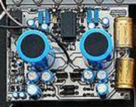
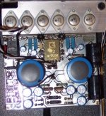
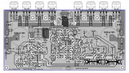
You guys are "EXPERTS" in grounding schemes and negative feedback traces, so can you please take the below picture (of Alex's current PCB layout) and draw in GREEN (Photo Shop, Paint, etc.) the correct ground traces (star ground, separate power and input ground, speaker out, transformer ground for 60VAC, etc.)? .......
I understand you simply don't care.
Why should I do pcb design for you?
Good luck with your pcb for the magic Goldmund amp.
")
If you look at the photo in post #140 you will see a STAR Ground, unless you are blind or do not want to see it.
Btw:
Yes, this looks like some partitioning of ground.
Resulution is way too low for an exact analysis but I can see something, too.
First things first. Please stop posting all these sources to prove your points to me. Trust me on this, I simply don't care. Those pretentious audio engineers, Ben Duncan, Douglas Self, etc. are no better than most audiophiles.
Here's a challenge for Lee Knatta, Tinitus, Jam, Krisfr, Jacco Vermeulen, and Ostripper:
You guys are "EXPERTS" in grounding schemes and negative feedback traces, so can you please take the below picture (of Alex's current PCB layout) and draw in GREEN (Photo Shop, Paint, etc.) the correct ground traces (star ground, separate power and input ground, speaker out, transformer ground for 60VAC, etc.)? And please draw the negative feedback trace in RED. Please use the original schematic attached bellow and do not add/alter any components, or remove the ground plane.
Since the experts are at work, maybe we can finish this PCB and get to the fun part. Which is building the amp!! Posting pictures!
this is a bit silly though. to be asking for a ground plane to be kept while suggesting that relatively basic grounding schemes such as star ground is humbug seems somewhat unreasonable. its a fairly well known scheme to use high current returns closer to the power supply filtering in order to reduce noise. the authors above are making some pretty valid scientific point on this that is taught early on at ee classes all over the world. if those guys are too pretentious then perhaps a fairchild semi note on star grounding is convincing? http://www.fairchildsemi.com/an/AN/AN-42036.pdf
i am actually quite interested in seeing what this can become, and i think it will be interesting to see how this could sound vs a similar topology combined with twenty years of engineering advances could do to it.
...but when i look the pictures of the pcb from the original i see some pretty deliberate layout choices and it appears that those choices arent carried over to this pcb. hence it i think it would border on the careless to simply dismiss the notion of at least carry the amplified return back closer to the power supply filters than to make it run across an entire pcb with mixed signal stages. the alternative us to pay attention in the layout for inference from the ground plane on sensitive stages -which i dont believe was part of this pcb design criteria but quite possibly something which goldmund could have paid attention to..?
in general i also like ground planes but not so much to send high currents through.
having said this it could very wellnbe that this wont matter much, thisbis why i think its important that someone builds one to validate it vs the design goals so that we know if the points raised are valid or not. ive done many designs in my professional career where some optimizations in the end just didnt matter, but likewise ive had experiences where some optimizations which shouldnt have mattered ended up making a huge difference.
so with that i suggest that go ahead and make one prototype and validate it. if its still the best youve heard then all others should go and build theirs. if it isnt then work with the community to improve it to make it to be the best that youve heard.
this is how i saw the dx blame evolution and i loved the iterative approach with lots of give and take in an engineering centric manner.
If I'm not mistaken the original design has the VAC on a separate board which is mechanically isolated from the main board. How can we call this a clone without doing this? Also, would placing this module on a separate board simplify the grounding scheme on the main board?
After coming across this thread a bit late maybe I've missed this somewhere in the previous 906 posts - maybe someone can point me to a relevant posts. If the idea is to clone a goldmund and capture the "magic" of a goldmund and the real thing is at hand, then why not clone the goldmund pcb layout? or at least the general arrangement modified as little as posible to accomodate modern components?
Surely cloning the schematic only is not going to lead to a clone of the amp?
Surely cloning the schematic only is not going to lead to a clone of the amp?
Tommy1000 - C20,C21,C22,C24,C25, and C26 (10nF/100V) capacitors were shown in more recent Goldmund schematics. Some amps had these, others didn't. In some Goldmund amps they were simply soldered to the bottom of the PCB. Without the caps, the amp could possibly oscillate, I would recommend installing them, they do no harm. But, it could also be something a potential builder can experiment with.
Msmart2b - It would be silly to make the A1 modules. Having the parts on the main PCB is the only way to do it for a simple DIY kit.
Bigpanda - If no one wants to improvise the grounding scheme, I think we are good to go with the group buy for Alex's latest PCB layout. I looked it over and there seems to be no mistakes
Given that I have learned a lot from this forum and to help those that have invested time and resources to this thread, I choose to lend some thoughts.
I feel for Alex IF he has to discard most of his Fine and honest work...
Nagys: Take a big bite of pie, humble will do. Show yourself that you are willing to LEARN
Now
Take note with a high def photo of the original board, notice the zones
Zone your board accordingly
duplicate the front end mod (with a small board if need be) in one of those zones
Put a Star ground point in the middle of the board
Establish an output Zone with larger traces for the supply lines
take a big fat ground trace from each zone to the star ground
No ground lines on solder side.
NOW The REAL experts can take what I have said & TEACH me a thing or 2
For those that want to modify the Goldmund schematics or post quotes from amplifier design books there is plenty of other threads for that. This one is about cloning the Goldmund as close to spec as possible.
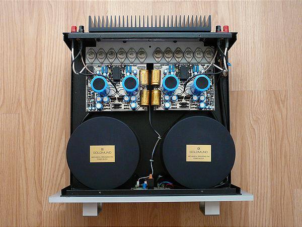
This is a very good question Nagys. Is there any chance of getting some high rez close up shots of the Mimesis 9.2 PCB ?
That pic that has been posted is of a Mimesis 6 stereo amp I think.
After coming across this thread a bit late maybe I've missed this somewhere in the previous 906 posts - maybe someone can point me to a relevant posts. If the idea is to clone a goldmund and capture the "magic" of a goldmund and the real thing is at hand, then why not clone the goldmund pcb layout? or at least the general arrangement modified as little as posible to accomodate modern components?
Surely cloning the schematic only is not going to lead to a clone of the amp?
This is a very good question Nagys. Is there any chance of getting some high rez close up shots of the Mimesis 9.2 PCB ?
That pic that has been posted is of a Mimesis 6 stereo amp I think.
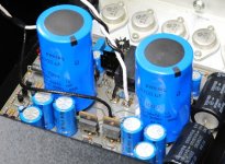
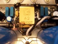
Ah, you can't see the star ground, or would you like to read the output device number ?
any more pics? BTW,It's a little different from the one in the post #140.
You mean the black 160V Siemens-B43 220uF axials instead of the Goldylock 250V Roederstein-EG series electrolytics ?
Other than that, only difference (i.c.s) are the additional TO-92 plate coolers for the Vas devices.
Speaking of Swiss perfection, the goldplated A2 upgrade modules didn't quite seem to fit without bending the drivers+TO18 Stargate heatsinks.
OopZie (Z = for Swiss accent).
The Telos monaurals and up are modular, see Telos 400 pic in post 902 ;
- Front end stage on a separate board right behind the inputs.
- Zoby coil soldered at the output terminals.
- AC carrying stuff as far away from the input as possible.
- Powersupply + protection circuitry on a separate board.
- Foil nF caps at the source of each output device.
(plus usual stuff as inrush limiter for the transformer, no rail fuses, other usual "audiophile" crapp)
Attachments
Last edited:
- Foil nF caps at the ..... of each output device.
Make that "Drain".
(i'm having a bad hair day)
The grounding "war"
Its a pity that those who have criticized the grounding and have pointed out alternatives don’t see any reason to contribute any longer about that question.
I can understand that Nagys stubbornness (sorry Nagys, but I really mean it) and rejection on your alternatives not to use only one groundpoint on the ground plane in earlier posts, have irritated you.
But in his post # 896 I felt a kind of "invitation" (yes, in Nagys very special way) and a admission that he was willing to listen to you, and for all I know, ask Alex for changes on the PCB.
Now I feel that the time has run out, and that I and all others that have ordered the PCB, have to accept a not optimal board.
Eivind Stillingen
- Home
- Amplifiers
- Solid State
- The Very Best Amplifier I Have Ever Heard!!!!