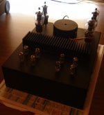
Here is preview of an amplifier that I've been collecting parts for, for a while now. The design is finalised, I just have to wait for the remaining bits to arrive and assemble the thing. The semiconductor complement is greater than the tube complement, so I guess this is the correct forum ")
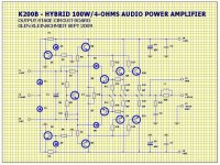
I've taken the standard 'Blameless' front-end a substituted all the icky-poo NPN's for loverly warm, glowing triodes. I've also added a cathode follower to buffer the VAS from the class-B double emitter follower output stage. This 12AT7 cathode follower is biased with a current source consisting of an identically connected (self-biasing) 12AT7, which effectively cancels most of the distortion of this stage.
I've simulated and optimised this whole design extensively in SPICE (shock! horror!) with accurate triode models and it works rather well.
All tubes in the input stage / VAS are 12AT7, except for the twin triode used for the LTP, which is a high gm 12AX7, as used in my K10A amplifier.
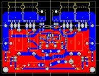
The input stage / VAS has a total of four twin-triode tubes and requires a power supply of +/-200V @ 35mA. These supplies are going to be provided by individual hybrid shunt regulators for each channel.
The four large tubes in the mock chassis layout picture are 807's, which are the shunt regulator elements, each of which cascode an NPN transistor control element. Four MTP2P50E P-ch MOSFETs mounted on a back-panel heatsink will be the constant current sources for the shunt regulators.
Shielded Chassis sockets will be used for the twin triodes.
The heater supplies for the twin triodes are regulated too. The 807 heaters are (sensibly) fed with AC.
Power up sequencing (heater warm-up/ HT timing /speaker relays, etc) and DC fault protection will be controlled by a PIC16F876.
I'll start etching the PCBs tomorrow evening…….
I've taken the standard 'Blameless' front-end a substituted all the icky-poo NPN's for loverly warm, glowing triodes. I've also added a cathode follower to buffer the VAS from the class-B double emitter follower output stage. This 12AT7 cathode follower is biased with a current source consisting of an identically connected (self-biasing) 12AT7, which effectively cancels most of the distortion of this stage.
I've simulated and optimised this whole design extensively in SPICE (shock! horror!) with accurate triode models and it works rather well.
All tubes in the input stage / VAS are 12AT7, except for the twin triode used for the LTP, which is a high gm 12AX7, as used in my K10A amplifier.
The input stage / VAS has a total of four twin-triode tubes and requires a power supply of +/-200V @ 35mA. These supplies are going to be provided by individual hybrid shunt regulators for each channel.
The four large tubes in the mock chassis layout picture are 807's, which are the shunt regulator elements, each of which cascode an NPN transistor control element. Four MTP2P50E P-ch MOSFETs mounted on a back-panel heatsink will be the constant current sources for the shunt regulators.
Shielded Chassis sockets will be used for the twin triodes.
The heater supplies for the twin triodes are regulated too. The 807 heaters are (sensibly) fed with AC.
Power up sequencing (heater warm-up/ HT timing /speaker relays, etc) and DC fault protection will be controlled by a PIC16F876.
I'll start etching the PCBs tomorrow evening…….
Attachments
Last edited:


I would suggest you to think on such things as:
1. Orientation of fins according to convection flow
2. Pentodes in CCS?
3. P-type triodes?
I used on labs analog computers, they had similar schematics of opamps in them. Without transistors, of course, but with gas discharge VR tubes for voltage shifts.
They had a couple of potentiometers for null adjusting: to balance a diffpair, and to adjust a null in an output stage.
The heatsink is big enough for the power to be dissipated, even in the vertical orientation.
The triodes (with heavy cathode degeneration) work quite fine in this application as constant current sources.
Show me a P-type tube!
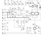
Another PCB (containing the DC fault detection comparators and balanced input circuitry) has a the DC servo's to steer the offset imbalance. That reminds me that I left out the servo return terminal on the input stage schematic & PCB. Oops.
The triodes (with heavy cathode degeneration) work quite fine in this application as constant current sources.
Show me a P-type tube!
Another PCB (containing the DC fault detection comparators and balanced input circuitry) has a the DC servo's to steer the offset imbalance. That reminds me that I left out the servo return terminal on the input stage schematic & PCB. Oops.
Last edited:
can you, please, remove it and post the schematic once again.
thanks in advance by your kindness,
regards,
Carlos
I'll post the full schematic in high res. B&W after it's built and tested; hopefully before the week is out.
The heatsink is big enough for the power to be dissipated, even in the vertical orientation.
Ok, it's yours, you may waste it for your pleasure.
But I am getting kind of a nervous reaction when see incompetently oriented heatsinks, like a tiger when somebody pets him in an opposite direction of his fur.
The triodes (with heavy cathode degeneration) work quite fine in this application as constant current sources.
Plain resistors will give as well blameless results.
Show me a P-type tube!
AFAIR, Demian (1audio) posted a picture of one.
Another PCB (containing the DC fault detection comparators and balanced input circuitry) has a the DC servo's to steer the offset imbalance. That reminds me that I left out the servo return terminal on the input stage schematic & PCB. Oops.
Oops, no "blameless" tag anymore.
Ok, it's yours, you may waste it for your pleasure.
But I am getting kind of a nervous reaction when see incompetently oriented heatsinks, like a tiger when somebody pets him in an opposite direction of his fur.
Plain resistors will give as well blameless results.
With a -200V powersupply, no, plain resistors "long tail" won't perform as well.
The LTP and VAS triode current sources are biased with a 20V zener diode and are cathode degenerated accordingly.
The 2.2mA LTP current source has a plate impedance of 580k.
The 5.1mA VAS current source has a plate impedance of 230k.
So, with a -200V supply, ~6 times higher impedance than fixed resistors to sink the same current.
The self-biasing current source for the cathode follower has a much lower plate impedance, of course, but this is entirely deliberate, as then gm variation of the CF CCS opposes the gm variation of the CF, cancelling (to a degree) the distortion (the CF has equal value cathode degeneration).
Last edited:
Member
Joined 2009
Paid Member
Progress on this build has been stalled a little because I decided to re-design part of it.
I want to have balanced inputs for this amp, and had originally designed a differential line receiver with a few fancy National Semi OPAMPs, which took up a circuit board separate to the input stage / VAS (front-end) circuit board.
I’ve now re-designed and simplified the differential line receiver using a Burr-Brown / Texas Instruments part and have incorporated it, along with the DC servo, onto the front-end circuit board.
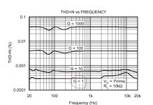
The part used is an instrumentation amplifier optimised for and intended for audio; part # INA217
Datasheet: http://focus.ti.com/docs/prod/folders/print/ina217.html
This IC has excellent CMRR and vanishing low THD throughout the audio band at the low gain settings. I’m using it here with a gain of 1.
Attached is a pic of the new differential input circuitry and the DC servo for my front-end PCB, and the THD graph for the INA217.
I want to have balanced inputs for this amp, and had originally designed a differential line receiver with a few fancy National Semi OPAMPs, which took up a circuit board separate to the input stage / VAS (front-end) circuit board.
I’ve now re-designed and simplified the differential line receiver using a Burr-Brown / Texas Instruments part and have incorporated it, along with the DC servo, onto the front-end circuit board.
The part used is an instrumentation amplifier optimised for and intended for audio; part # INA217
Datasheet: http://focus.ti.com/docs/prod/folders/print/ina217.html
This IC has excellent CMRR and vanishing low THD throughout the audio band at the low gain settings. I’m using it here with a gain of 1.
Attached is a pic of the new differential input circuitry and the DC servo for my front-end PCB, and the THD graph for the INA217.
Attachments
Progress on this build has been stalled a little because I decided to re-design part of it.
ICs and tubes, you must have a lot of fun. I certainly do, watching people anxiously waiting for the full schematics

May I suggest discharge tubes, replacing those icky zeners, they will certainly improve the sound.
The "icky" comment was a joke.
Don't worry, mine was a joke as well. Discharge tubes are much noisy than zeners - but they look cool with that purple light.
A couple of magic eye tubes may add to the coolness. Alternatively, may I suggest a CRT in the VAS?
I already have one (of a collection) DG7-32 75mm CRT put aside for another amp, but that will be used as a signal monitor.
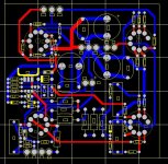
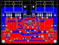
Revised "front-end" pcb layout all done, bubble etch tank awaits........
This board mounts directly under the top of the chassis and is supported entirely by the four chassis-mount valve sockets (which are soldered to the side of the PCB opposite to all the other components).
Revised "front-end" pcb layout all done, bubble etch tank awaits........
This board mounts directly under the top of the chassis and is supported entirely by the four chassis-mount valve sockets (which are soldered to the side of the PCB opposite to all the other components).
Attachments
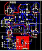
Revised "front-end" pcb layout all done, bubble etch tank awaits........
How do you transfer layout on copper clad?
How do you transfer layout on copper clad?
Positive acting presensitized PCB, a Kinsten UV light box, inkjet transparancies, sodium metasilicate and warm water.
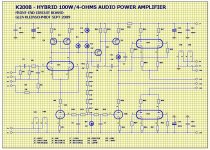
Revision #2; Forgot the catch diodes on the OPS schematic.

Oh well, it should be easy enough to solder/fudge those onto the underside of the PCB.
Attachments
Last edited:
I'm just blogging as I build the thing. I'll be playing PCB-loading on the weekend. I'll get all the interconnected boards up an running rats nest on the bench top before I bother stuffing the lot into the chassis, all 12 transformers and all.
Full schematics with component values will be posted when it's operational and tested...............................and some of the more straight forward ones in the mean time, as time becomes avaliable to draw them all nice and pretty in the 'puder cad thingie, that is.............
Full schematics with component values will be posted when it's operational and tested...............................and some of the more straight forward ones in the mean time, as time becomes avaliable to draw them all nice and pretty in the 'puder cad thingie, that is.............
- Status
- This old topic is closed. If you want to reopen this topic, contact a moderator using the "Report Post" button.
- Home
- Amplifiers
- Solid State
- A tubular 'Blameless'