Elektor amp 5/97 output stage
Have you seen this kind of output stage and how do you feel about this? (think IGBT into bjt or MOSFET)
I think there are several plusses here. One can set the output stage for 2X or 4X voltage amplification for example. This in turn means that voltage amp stage does not have to have as much voltage swing and can be cascoded or have a stabilised supplies taken from primary supply....
And then think if there would only be the final and driver stage which would form a power amp with 14-20X voltage gain..... A friend of mine came up with such circuit and it's in my next four months or so todo list")
Ergo
Have you seen this kind of output stage and how do you feel about this? (think IGBT into bjt or MOSFET)
I think there are several plusses here. One can set the output stage for 2X or 4X voltage amplification for example. This in turn means that voltage amp stage does not have to have as much voltage swing and can be cascoded or have a stabilised supplies taken from primary supply....
And then think if there would only be the final and driver stage which would form a power amp with 14-20X voltage gain..... A friend of mine came up with such circuit and it's in my next four months or so todo list
Ergo
Attachments
Elektor amp 5/97 output stage
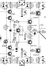
I've no seen anything quite the same as this before but it looks like a variation of the Class A+B topology. T15 and 16 look to be a fairly standard output stage (probably class AB) whilst T16 and 17 presumably provide additional (Class B?) power. I note the somewhat unusual inclusion of R30 though, which I assume allows T16 and T17 to provide voltage gain too. It is this aspect that I regard as the most novel.
Note that the driver is already cascoded by T12 and 13.
Ian.
IAN McMILLAN
Here is the information you requested. Also look at my earlier thread to Alaskanaudio. The imput stage, consisting of a differential transistor pair TR1 & 2 and a current mirror, TR3,4, converts the differential imput voltage to a single output current. This current feeds the base of driver transistor TR9 and via the common base transistor TR8 feeds the base of the driver transistor TR10. The driver transistors supply their emitter currents to power transistors TR11 and TR12 respectively. Biasing and Class-AB control are achieved by means of a bias-control loop formed by TR6-9. Due to the buffer function of TR6 the base-emitter voltage of the power transistor TR11 is isolated from the bias control loop. This is done to avoid thermal or HF switching distortion problems mentioned earlier. This design is based on complementary/pnp transistors. Their parameters can be assumed equal to make the equations easier. The Class AB control is based on the well-known geometric Class AB control law. Ic8 x Ic9 = I²r (2) The DC collector current of the driver transistors is given by Ic9 = Ic10 which = Ir x the square root of HFE (3).
Collector terminals of the driver transistors TR9,10 connect to the output terminal to minimize driver dissipation and to prevent the power transistors TR10,12 from saturating. Power dissipation in the bias-control loop transistors is low compared to the dissipation in the output transistors. Hence, if TR6-9 share a small heat sink, thermal stability is achieved without emittor degeneration and switching distortion. The remaining dominent source of temperature dependence is the temperature coefficient of the power transistor forward current gain. This coefficient is approximately 0.6%/K to the power of 4. Maximum output current is determined by emitter current and the current gain of TR9,11 or TR10,12 respectively, Io (max) = plus or minus Ieh²fe (4).
It can be seen that, in contrast with many other designs, the maximum output current capability is symetrical. A problem with power transistors driven by a current source is that there is no turn-off resistor for them. Under high frequency, high-amplitude drive there will be a tendency for the effective bias current to rise dynamically. By using HF power transistors with a ft of 80MHz, this bias current rise is reduced to 60% at 20kHz at full drive.
In summary this Class AB common-emitter power amplifier incorporates a new current mode Class AB driver circuit to obtain good thermal stability of the quiescent current in the output stage. It also guarantees none-zero currents in the output transistor that is conducting the resisdual current, avoiding HF switching distortiion. Maximum output voltage is near to the rail-to-rail limit. Saturation in power transistors is avoided, resulsting in fast recovery from clipping. The circuit has an excellent stability due to a phase margin of 85 degrees with a B 1/34. There is more but I hope that this gives the salient points. So Ian all we need now is for you to put a su/sy on the front pretty please.
Elektor amp 5/97 output stage
Output stage voltage gain is approx (R30+R29)/R29. Snip out R29 and s/c R30 and the gain drops back to unity. The ETI-480 amp used such a configuration but with bipolar outputs. I would expect the higher the gain the more critical the bias setting, i.e. you wind the pot to get some current and when it does start you would only have to *look* at the pot and it would alter the current a fair bit, depending on the gain.
GP.
Common source etc
Another advantage of the gain in the power stage is that the signal swing in the voltage amplifier stage is reduced. In this amp, it allows them to feed the Vas with an LM317/337. This makes for very cheap and simple stabilised supply for the pre-stages, rather than a more complex 40 or 50V stabilised supply if the output stage didn't have gain. Could that be actually the reason they put in the output stage gain?
Cheers, Jan Didden
new class AB power amp
AMPMAN, I've now read your explanation of how the above circuit works pretty thoroughly. I get the general jist but sadly can't claim to have understood all the details. In particular I not't know to what the "r" in the various corresponds. I studied Electronics at college but that was a long time ago. Also you say that the bias control loop comprises Tr6-9. Did you mean this or should it be TR5-8? I have to admit that BJT and current-mode operation give me a headache. I'm more comfortable with FETs and voltage mode. Fortunately I also happen to prefer the sound of the latter, at least in general.
I also missed your plea for SuSy front end on the first reading. In principle this would not be difficult but I fear that practice might well be very different. SuSy requires simple circuits and this one does not really qualify. However, if you wish to try, simply follow the principle in the Aleph-X thread since the general topology of this and an Aleph are similar. You will of course have to produce a bridge design, i.e. replicate the output stage. Also the current mirror on the front end will have to go, or be modified since you will require both output phases. If you decide to go ahead then I wish you the best of luck. BTW, I'm not the expert on SuSy. Perhaps you had better ask Nelson (as the inventor) for his opinion?
Ian.
Ampman
sorry but only now i can anserwer you, because i´m was far from home all this week.
Regarding the schematic i already know it because i´m a long time reader of Electronic Wireless World. It´s in fact a realy enovatif disign but what i have said regarding ampilfiers with high open loop output impedance i still mantain it.
When you talk about the article by Robert Cordell, i don´t know it, but i don´t belive in everythig that is written.
If you can prove my point make that experience with your amplifier.
- connet another amplifier through a 8 Ohm resistor to the output of your amplifier...Put some signal in the other amplifier and put the prob point of a osciloscope in the collector of Tr1.
you will see that the same signal is bieng amplified by your amplifier in reponse of a disturbance in the output.
Thats what i said about the intermodulation betwen the original signal and the reaction from the speaker.
But you d'ont need to belive me because i d'ont write in EWW.
regards
Jorge
AMPMAN
One more point!
When you said that your amp have 0,030 Ohm output impedance and because that it will not be subjected to interface intermodulation distortion you are forgetting that, that impedance is obtained from the feedback . So as the open loop is very high the reactions from the speakers "fell free" for reaching the input LTP ...the ideal conditions for the interface intermodulation distortion to happen...this is not new...as i said Matti Otalla also have remarked that many years ago...
Regards
Jorge
TubeDude
I hate to say it but a common collector will be subjected to the same phase shift in another way. The phase shift will show up in the previous stage.
A bipolar Junction Transistor is in general a current - current converter which in the perfect world is a linear transfer slope. So on the base of a BJT the phase shift will show up. Not as large but it will be there.
So if you Feedback loop has to compensate for the phase shift on the output or a phase shift in the the VAS stage because of a capacitive load.... This will be be the same result.....
Only a Common Emitter stage will be subjected to saturation. and it should be easier to control/minimize those swith glitches presented by class B and AB mode.
Sonny
In common collector/emitter one of you Transistor will turn of and create switch glitches.
Both circuits will have the same control over the speaker when they have the same output impedance, frequency response and phase margin..
Only then you wil be able to compare those two types of output stages.
Sonny
Both circuits will have the same control over the speaker when they have the same output impedance, frequency response and phase margin..
Only then you wil be able to compare those two types of output stages.
Sonny
tube dude
I quote cordell directly, Interface intermodulation was next measured in a manner equivalent to the procedure outlined in reference 1. Equal-level 1000 and 60Hz signals were applied to opposite ends of an 8 ohm load resistor by the amplifier under test and a second power amplifier. A spectrum analyzer was placed across the output of the amplifier under test and the R.M.S. sum of the distortion products was referred to the 1kHz level. The operating level of each amplifier was 25W. The similar levels of interface intermodulation in all 3 cases confirm that open-loop output impedence and feedback factor have virtually nothing to do with it in amplifiers properly constructed at the same cost.
This is the summary of a highly detailed and exhaustive analysis investigating interface intermodulation by an expert in this field.
Ampman,
Have you actually built the circuit (of the schematic posted in this thread) from EW&WW using 2SC5200 and 2SA1943 transistors? How does this amp sound?
As a starting point, I built this amp soon after publication of the article and since the output devices were not available(even then), I used MJE3055/2955 transistors. Soon after powering up, the bias shot up and blew the output devices. Although I had to hand, quite a large number of 2SC3281 and 2SA1302 transistors, I did not try the amp with these. I thought that the 60MHz fT criteria was quite critical to the stability of the design while the transistors I had were only about 30MHz, and gave up completely on the design.
Input from your success may cause me to give this amp a try again. Thanks.
Member
Joined 2009
Paid Member
An interesting output stage that strangely, hasn't generated very much follow-up on this forum, no Spice, no builds or anything ?
My tssa is just such an design, and is Working very well.
Drain follower Can compete with the very Best source follower designs.
Member
Joined 2009
Paid Member
- Status
- This old topic is closed. If you want to reopen this topic, contact a moderator using the "Report Post" button.
- Home
- Amplifiers
- Solid State
- Common Source versus Common Drain output stages