OK.
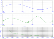
As diyMartin observes, the amp is severely underbiased (in fact there is zero bias current) so there is huge crossover distortion. See THD residue and harmonics.
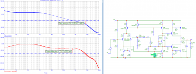
So, running an AC simulation with no output current gives misleading results, since the power transistors are off. So I add a current source in the output and step it from -2A to +2A.
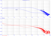
As the sim shows, with 0 output current the amplifier is basically off, so it is stable, but with non zero output current, it is unstable.
This has nothing to do with the input stage btw.

As diyMartin observes, the amp is severely underbiased (in fact there is zero bias current) so there is huge crossover distortion. See THD residue and harmonics.

So, running an AC simulation with no output current gives misleading results, since the power transistors are off. So I add a current source in the output and step it from -2A to +2A.

As the sim shows, with 0 output current the amplifier is basically off, so it is stable, but with non zero output current, it is unstable.
This has nothing to do with the input stage btw.
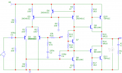
I add a current mirror on the input stage to fix the unbalanced currents noted by previous posters, and a protection transistor on the VAS, and I set the bias to 50mA by adjusting resistors on the Vbe multiplier. The amp is still unstable, but now it is visible, instead of being hidden, since the transistors are now on when output current is zero.
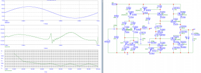
Also like all CFP output stages the output devices can't turn off properly, which is kind of a problem. See current through both power devices, turnoff is much slower than turn on.
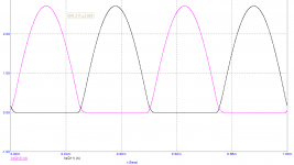
If you test at 100kHz, or run a slew rate test with a square wave, or if it oscillates, since the transistors can't turn off fast enough, they conduct at the same time and explode.
Now, previous AC simulation shows it is unstable when the top power transistor conducts, but not when the bottom power transistor conducts. Since the compensation cap is connected to the side that is stable, this is suspicious.
So I add a 1µF cap across the Vbe multiplier, and now the AC sim looks a lot nicer. I also change the CFP resistors from 2k2 to 100 ohms so the drivers have some bias to work with, and readjust the Vbe multiplier for 50mA bias.

Also like all CFP output stages the output devices can't turn off properly, which is kind of a problem. See current through both power devices, turnoff is much slower than turn on.

If you test at 100kHz, or run a slew rate test with a square wave, or if it oscillates, since the transistors can't turn off fast enough, they conduct at the same time and explode.
Now, previous AC simulation shows it is unstable when the top power transistor conducts, but not when the bottom power transistor conducts. Since the compensation cap is connected to the side that is stable, this is suspicious.
So I add a 1µF cap across the Vbe multiplier, and now the AC sim looks a lot nicer. I also change the CFP resistors from 2k2 to 100 ohms so the drivers have some bias to work with, and readjust the Vbe multiplier for 50mA bias.
Ha ha. Lowering the simulator timestep removed the bursts of oscillation, which means it was just a transient simulation artifact. So, the AC stability analysis was correct. And that pointed to the problem being way too little bias both in the output transistors and the CFP drivers.
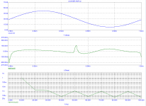
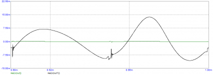
I set it to emitter follower instead of CFP, which gives much lower crossover spikes. Also, in an emitter follower configuration, the output transistors turn off much faster, so they explode a bit less.
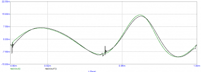
Green is emitter follower distortion residual, black is CFP.
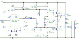
Mistake on schematic, VAS is BD139.
I set it to emitter follower instead of CFP, which gives much lower crossover spikes. Also, in an emitter follower configuration, the output transistors turn off much faster, so they explode a bit less.

Green is emitter follower distortion residual, black is CFP.

Mistake on schematic, VAS is BD139.
Last edited:
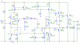
Polishing:
- Darlington VAS
- TMC
- Inductor in the input pair for 3rd order compensation "special Swiss sauce" (got that recipe from Groner in Linear Audio)
Should be a difference in parts cost of about $1
I'll bet a beer that if you replace the CFP with a classic emitter follower (and add a zobel) your transistors will stop exploding.
- Darlington VAS
- TMC
- Inductor in the input pair for 3rd order compensation "special Swiss sauce" (got that recipe from Groner in Linear Audio)
Should be a difference in parts cost of about $1


I'll bet a beer that if you replace the CFP with a classic emitter follower (and add a zobel) your transistors will stop exploding.
1. Short the base of the drivers so that no current flows in output.
2. Disconnect feedback from output and connect to shorted bases. This creates a signal amplifier.
3. Check emitter currents of input pair by measuring volts across emitter resistors.
4. If input imbalance persists, remove R29 470 ohm from feedback to create unity gain amp. Is C8 100uF leaky?
5. Debug in signal mode first before re-connecting outputs.
Ok so. I tried to isolate Better my circuit and add some more Miller Comp to the vas stage. I even replaced my CCs resistors and supermatched the input stage so no assymetry. The schematic Is the First i poster with the CFP output stage
I raised the differential degenerating resistors to avoid the likehood of oscillations . I even out a 470picofarad in parallel ti my 10k feedback resistor . So i tried to probe the circuit without the output stage. Only the differential and vas stage assuming that closing the feedback ring onto my CCS would give me good resoults. And It did!. The vas stage was biased properly and no issues whataoewer with noise or other things(i got noise but It gets amplifier by the vas stage from 10mv to 100mv so not a real problem) And i tried hooking my output stage. So when the output stage Is with no Bias (class B) in cutoff the feedback gets to amplify that noise and from 100mv i get almost 5v (this doesnt happen when i connect the supply but its like an oscillation trigger, when some time has passed It starts to do it) and i suppose this 5 volts are limited by the resistors i put in series with the Power supply ti limit the current . On the other Hand when i do class AB and i put at least 10ma trough the output stage all of this vanishes and the amplifier Is beautifil and stable. There we come ti the final problem. Wich is when i disconnect the resistors and i directly Power the amplifier . The output stage explodes again . Can i Say? Wtf?
K wtf?
What Is the problem now. Do i have to believe that i cant use this CFP output stage? Because the purpouse im using It Is because its really efficent and It can be driven with 1/10 of a darlington or emitter follower output stage . Thank you veryuch 😉
It's refreshing to see the Blow-by-Blow fight and struggle that you have narrated here. Solid state design requires a commitment to fundamentals that might be just out of the reach of the casual hobbyist. I've been successful and happy with tinkering with tube based designs over the decades because you only need simple AC theory to get you through. Tubes can also be abused and the breadboard circuits will still work. I've done some bad things to tubes, but still had viable components to complete the goal. It seems to me that in order to be successful with solid state, perhaps 4 to 6 classes in the Electrical Engineering Department will give you the groundwork to tinker. At that point, might as well get another degree!
Nice
I Also got experience in tube circuits as you said they are Easy to design and to realize.
I know its hard to make solid state Amps and that this Is not a joke.
I Also got experience in tube circuits as you said they are Easy to design and to realize.
I know its hard to make solid state Amps and that this Is not a joke.
1. The biasing transistor Q2 has too little current into the base. The base-emitter resistor should be 2.2K. Adjust base-collector resistor to suit. BD139 may be better as it can be bolted to same heatsink as power devices for thermal compensation.
2. Check that the signal version with a sine signal looks correct.
3. Check the signal version with a square wave. Adjust compensation to give fast rise time but no overshoot.
4. 470pF across feedback resistor is too big. Larger values introduce instability. 10pF and under maybe.
5. If signal is amplified correctly remove the power transistors and use the driver transistors as emitter follower output but change 0.22R resistors to 22R 1W. If the amp goes unstable these will blow but the transistors should survive. Put 220R in series with the bases of the drivers.
6. Retest with sine and square wave and readjust compensation.
7. Add input filter with 470R in series with input and 220pF to ground. The input coupling capacitor should be after the filter to keep the volts on the cap low.
8. If the driver version works, add the power transistors. Slowly reduce 22R in emitters when stable.
- Home
- Amplifiers
- Solid State
- Differential amplifier understanding
