Good evening to everyone.
I started this post because i got some problems in designing my class Class AB amplifier, in particular the differential input stage.
the amplifier is running with a single supply of 50v and therefore the problem i encountered in my input stage:
i tried to understand and look ad other schematics that use the differential input stage with a single supply or at opamps such as lm324 wich on his input has a differential amplifier connected from positive rail to ground.
the problem is that when i use softwares as ltspice or pspice to simulate my circuit everything seems fine , the frequency response and the attenuation of peaks and high frequency oscillation is beautiful.
when it comes to reality when i build my differential input stage such as the schematic 2 things happen.
first of the output of the driver transistor goes to all the way to ground or vcc and this causes my Vas stage to not be centered and claim current trough my upper ccs wich causes the output stage to explode in a loud and visibly spectacular explosion.
on the other hand when i bias the bases of the output transistors by lifting up the ground trough an equal resistor divider the amplifier works fine but the feedback applied by the differential changes from what i calculated using the softwares. i want to really know why because i tryed many many polarizations and configurations but i still get the same problem. i'l post the schematic.
Thanks very much and sorry for my bad english
An externally hosted image should be here but it was not working when we last tested it.
Like this for images 🙂
How to attach images to your posts.
Have you tried:
1/ A Zobel network at the output together with the usual inductor before the load.
2/ Add a small compensation cap across the feedback resistor.
3/ Making the input arrangement a little more sophisticated both in terms of the DC biasing and also adding a filter.
If you attach your .asc file (it will attach directly to the forum) then we can take a look.
Attachments
next i will try it but i think the zobel network and the inductor wont help much. because it has this problem with and without the load connected or varying the output impedance of the load . i get the same results. as i said earlier when i lift the base of the second transistor wich does the feedback connecting it to the resistor divider the amplifier works with no explosions but the feedback is totally wrong.... 😕
Attachments
A Zobel network could help massively... it is pretty much essential for stability 🙂
Use a bulb tester in your power supply to prevent damaging explosions... it will limit the current. Use a low wattage filament bulb to begin with.
Your simulation file (the .asc file LTspice uses) will attach just the same an an image if want to share it.
Use a bulb tester in your power supply to prevent damaging explosions... it will limit the current. Use a low wattage filament bulb to begin with.
Your simulation file (the .asc file LTspice uses) will attach just the same an an image if want to share it.
Complementary feedback pairs (or Sziklai) are more tricky and prone to oscillation than darlington ones. You might take a look at R. Elliott's P3A for potential solutions.
next i will try it but i think the zobel network and the inductor wont help much. because it has this problem with and without the load connected or varying the output impedance of the load . i get the same results. as i said earlier when i lift the base of the second transistor wich does the feedback connecting it to the resistor divider the amplifier works with no explosions but the feedback is totally wrong.... 😕
Is Q15 the 'second transistor'?
You are using a capacitor between the amp and speaker? As shown, if you do not, you might get the result you are talking about.
I tried a lot of things. And i really think the amplifier does not have oscillating problems. I tried ti Power It up with a bench Power supply and the really really strange thing Is that when i Power It up below 18-19v VCC the thing works great . But any voltage up 18-19v and the amplifier Just goes into short circuit wanting to draw lots of current. It couldn't be the bias because i even removed the vbe multiplier and runned the output stage in class B config to troubleshoot further
I discussed this problem with others Friends and we all have the same problem , its ridicoulous because all simulators and even theory Tells us this schematic should work fine but It doesnt.. i wonder what happens when i raise the supply up to 19v .
I discussed this problem with others Friends and we all have the same problem , its ridicoulous because all simulators and even theory Tells us this schematic should work fine but It doesnt.. i wonder what happens when i raise the supply up to 19v .
Attachments
Is Q15 the 'second transistor'?
You are using a capacitor between the amp and speaker? As shown, if you do not, you might get the result you are talking about.
Yes q15 Is the second transistor im talking about. Im Sorry for my bad english 😱.
And yes when connecting to a load because my offset Is half the supply im using not only a capacitor but 2 antiparallel capacitors
I'll take a look at the .asc later 🙂
Two 'anti parallel' caps doesn't sound good. Maybe the meaning is wrong. One would be reverse biased......
Two in series either plus to plus or neg to neg would work but are definitely not needed on a single rail amp. A single polarised cap is always the best choice here.
Two 'anti parallel' caps doesn't sound good. Maybe the meaning is wrong. One would be reverse biased......
Two in series either plus to plus or neg to neg would work but are definitely not needed on a single rail amp. A single polarised cap is always the best choice here.
Have to say it is a lot better than I was expecting. Bias set to 10 ma here. There are things I would alter but it is off to a decent start 🙂
I know from past experience that good layout and grounding is absolutely vital and that these designs can go unstable at the drop of a hat.
I know from past experience that good layout and grounding is absolutely vital and that these designs can go unstable at the drop of a hat.
Attachments
Well what can i Say. To ensure the most stable ground connections and to be Shure the circuit Is not affected by any noise (there Is but its 2mv and gets amplified to 20-40 by the vas stage wich is pretty low and can be even noise from the probes) i connected the ground of the circuit to the common earth connection of my house (i live in Italy i have earth connection) wich in most cases with amplifiers solved the problem.
But now It seems to not have any effect and the behavior of the circuit Is still the same . I tried and did my best to ensure the stability of the circuit and eliminate all flaws . I even added small 100pf capacitors on the bd139 bd140 output stage driver and in pspice this gives me a flat frequency response and seems to lower the High frequency gain further eliminating the probability of oscillations problems. What can i Say ? I was wondering about schmitt trigger behavior or the differential input stage . because its really really strange that the circuit at a certain VCC voltage Just Pulls everything to short circuit
But now It seems to not have any effect and the behavior of the circuit Is still the same . I tried and did my best to ensure the stability of the circuit and eliminate all flaws . I even added small 100pf capacitors on the bd139 bd140 output stage driver and in pspice this gives me a flat frequency response and seems to lower the High frequency gain further eliminating the probability of oscillations problems. What can i Say ? I was wondering about schmitt trigger behavior or the differential input stage . because its really really strange that the circuit at a certain VCC voltage Just Pulls everything to short circuit
I will try and have a closer look at your simulation file tomorrow 🙂
(You might find increasing the gain does help. Try reducing the 470 ohm as a test. And add a Zobel 😉)
(You might find increasing the gain does help. Try reducing the 470 ohm as a test. And add a Zobel 😉)
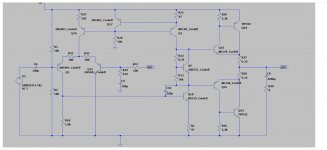
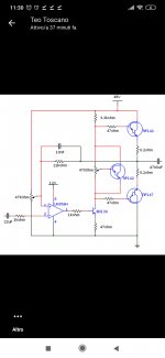
Sorry that I just jump into this - but having made a quick DC analysis, I may want to question the design.
There definitely may be issues with stability - but:
The design aims at keeping the DC output at the same DC voltage as the center of R2 and R3 (I know - I am stating the obvious, sorry) - that is half the supply.
In this state it would be expected that Q1 and Q18 will draw the same current (basically determined by Vbe of Q17 divided by R35) - that is around 12.8 mA.
That would also imply that the base voltage of Q18 relative to gnd will match Vbe of Q17 + Vbe of Q1: 1.2V-1.3V should not be far off.
Assuming a beta of 100 in Q18 the base current in Q18 will therefore be around 128uA.
The current through R24 will be the base voltage of Q18 divided by 1.8K - ca. 720uA.
This means that the collector current in Q3 will be 128uA + 720uA - that is 0.85mA.
The total current in the differential input pair is the collector current in Q16, and that is approximately determined by Vbe of Q17 divided by R27 (assuming equal Vbe in Q16 and Q1) - that would be around 0.6V / 220 Ohm = 2.7mA
This means that Q15 will carry around 1.9mA where Q3 would carry 0.85mA.
This is not a input stage in balance and I would consider lowering R24 to 1K.
But: this is probably not the problem you face, as it should still work.
Another observation: the Vce of Q2 will be rather close to Vbe of Q2 - given the current this may be up to 0.7V (this is caused by the very small value of R32 compared to R33).
This means that the two driver transistors (Q22 and Q25) will share 0.7 for biasing - that is 0.35V each, basically keeping both transistors in cut-off.
That will not allow any reasonable idle current through Q23 and Q24.
So, even if other issues are solved, the amplifier will therefore suffer crossover distortion.
Note: Having transistors exploding is a not-so-seldom result of mixing up the leads - that is connecting a transistor the wrong way.
Cheers Martin
Sharing Q17 between Q1 and Q16 is not a good idea. When Q18 cuts off to send the output to the positive rail, there is not current for Q1 so Q17 tries to maintain the current and that affects the current in the input pair. Better to replace Q17 with two diodes.
Im really trying to understand how opamps such as the lm358 are used as differentials input stages such in this example schematic that i found online... But in missing something . I think the polarization of the bases of my differential Is not correct... The simulation softwares Say that everything Is working but in reality Is not.. im confused😕
Attachments
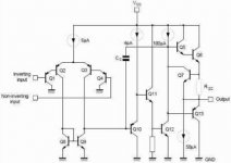
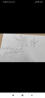
Looking at your diagram I would quickly say that the opamp inputs are the wrong way around and that the preset should be biasing the + input which would then be the signal input.
On a practical level the opamp must operate its output at around 500mv above ground to operate the VAS transistor and I doubt the 358 in practice could do that.
Get the inputs sorted and try feeding the opamp output direct into the base of the TIP147 output and omit the VAS transistor.
On a practical level the opamp must operate its output at around 500mv above ground to operate the VAS transistor and I doubt the 358 in practice could do that.
Get the inputs sorted and try feeding the opamp output direct into the base of the TIP147 output and omit the VAS transistor.
The amplifier oscillates.
im really confused . because i have read a lot of books and posts about designing this really simple amplifiers but no one really explain to you in easy words how to do the biasing of the various stages. on double supply the circuit seems to work but in single it doesnt wanna work at all and im going mad....
i read a lot of things and they always explain you a little bit of theory and then a whole odissey about how these things work based on temperature (wich is ok and i understand that these devices got thermal runaway) but i dont wanna know how thermal runaway affects these circuits because i dont go crazy on the SOA of the devices. the more i dig deep the more i seem to get confused. the post is entitled differential amplifier understanding and i really wanna know how it works in single supply. an example of a circuit already polarized and with calculations on how to calculate the resistor and what voltage and in what circumstances i expect to find certain voltages in certain points...... this whole thing about feedback leads me always to oscillation. im not trying to create a schmitt trigger but an amplifier....
if there is some willingful and nice person that wanna help me i can provide in private some other contacs like my whatsapp or facebook diving further into this rabbit hole. thank you very much for the help. i just dont wanna believe im brain dead XD
On two of the schematics of post #15 there is no DC path for bias current to the minus (-) input of the opamp.
Oscillation often means too high inductance in the layout and wiring.
Post a picture of your build.
Post a picture of your build.
- Home
- Amplifiers
- Solid State
- Differential amplifier understanding