Hello. This is my first post on diyAudio. I am not a "tech", just a guy who has been tinkering with stereo equipment for the past few years and trying to learn what I can. I have been successful at repairing/restoring several Carver pieces and I was able to repair an NAD 2140 and NAD 3140, both which were DOA due to shorted output transistors and a host of other problems. I am just learning to use an old Tektronix 2205 scope.
I am trying to fix an NAD 3020 series 20 with a distorted right channel. This unit has the four main power supply caps in the center of the board. I have confirmed that the distortion is in the amp section. I started by replacing the electrolytic caps in the power supply sections and the preamp and amp. DC offset can be adjusted to very near 0 mV. This made no difference. Power supply voltages seem reasonable. I touched up some suspect solder joints and checked that there were no continuity problems. Some work has been done previously on this unit, namely replacement power supply caps but everything used was under spec so I replaced them. The solder pads on this unit are very fragile. I replaced the 20k ohm variable resistor for the dc offset and I replaced the fixed bias resistor with a bourns 1K ohm variable resistor.
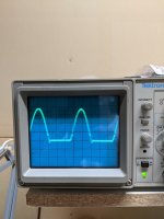
I used an online tone generator for a source and I had an 8 ohm dummy load connected to both channels. The right channel output shows that the negative half of the sine wave is clipped. (sorry, I don’t know how to insert pics into the body of the text so I will attach at the end)
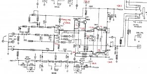
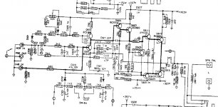
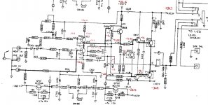
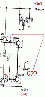
I disconnected everything and I went ahead and measured some voltages to compare to the schematic. Voltages are way too negative. (example, the base of Q610 is measuring about -13V instead of -0.6V) I have included the schematic for the left channel for specs and the schematic for the right channel with proper voltages in black and my measured voltages in red.
There didn’t appear to be any shorted transistors. Resistors seem Ok. I replaced a few just for the heck of it. No shorted ceramic caps. Not knowing exactly how to proceed, I went ahead and changed out Q602, Q604 and Q606 one at a time. No difference. Did the same with Q608, Q610, Q612 (replaced the 2sd669 with KSC2690). No difference. Replaced Q614 (used KSA1220 to replace the 2sb649). No difference. Well then something inside of me said to connect the dummy load again and take new measurements. Surprisingly, the voltages now read correctly! (at zero volume) BUT…. If I put a signal back in and slowly turn up the volume, the voltages quickly go too negative and the output is still clipped.
I have exhausted by limited knowledge at this point. I cannot figure out why the right channel has this excess of negative voltage. It must be something either horribly complicated or dirt simple. Any help or ideas would be much appreciated. Hopefully this all makes sense. Thanks for taking the time to read this post.
I am trying to fix an NAD 3020 series 20 with a distorted right channel. This unit has the four main power supply caps in the center of the board. I have confirmed that the distortion is in the amp section. I started by replacing the electrolytic caps in the power supply sections and the preamp and amp. DC offset can be adjusted to very near 0 mV. This made no difference. Power supply voltages seem reasonable. I touched up some suspect solder joints and checked that there were no continuity problems. Some work has been done previously on this unit, namely replacement power supply caps but everything used was under spec so I replaced them. The solder pads on this unit are very fragile. I replaced the 20k ohm variable resistor for the dc offset and I replaced the fixed bias resistor with a bourns 1K ohm variable resistor.
I used an online tone generator for a source and I had an 8 ohm dummy load connected to both channels. The right channel output shows that the negative half of the sine wave is clipped. (sorry, I don’t know how to insert pics into the body of the text so I will attach at the end)
I disconnected everything and I went ahead and measured some voltages to compare to the schematic. Voltages are way too negative. (example, the base of Q610 is measuring about -13V instead of -0.6V) I have included the schematic for the left channel for specs and the schematic for the right channel with proper voltages in black and my measured voltages in red.
There didn’t appear to be any shorted transistors. Resistors seem Ok. I replaced a few just for the heck of it. No shorted ceramic caps. Not knowing exactly how to proceed, I went ahead and changed out Q602, Q604 and Q606 one at a time. No difference. Did the same with Q608, Q610, Q612 (replaced the 2sd669 with KSC2690). No difference. Replaced Q614 (used KSA1220 to replace the 2sb649). No difference. Well then something inside of me said to connect the dummy load again and take new measurements. Surprisingly, the voltages now read correctly! (at zero volume) BUT…. If I put a signal back in and slowly turn up the volume, the voltages quickly go too negative and the output is still clipped.
I have exhausted by limited knowledge at this point. I cannot figure out why the right channel has this excess of negative voltage. It must be something either horribly complicated or dirt simple. Any help or ideas would be much appreciated. Hopefully this all makes sense. Thanks for taking the time to read this post.
Attachments
Last edited:
Agreed wiseoldtech. And i did compare the left and right channel and the only thing I find different is these voltages. Its a 40 year old amp so I figured capacitor replacement was a good start. Changing out the transistors was easy to do and I already had them in stock from previous NAD projects. Believe me, I did not want to try a blanket shotgun approach to repairing this unit, I just can't figure out where this voltage problem is coming from.
As for not having knowledge or training, well we all have to start somewhere.
As for not having knowledge or training, well we all have to start somewhere.
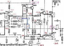
The place where the problem starts is often the place where the bad part is. The problem seems to start a the junction of R638 and R642. I'd check the values of all those resistors around there. C630 or C628 may be leaking.
You could also have negative current leaking into the junction of R638 & R642 through flux on the board, or a component lead bent across and touching another trace, or something like that. You clean flux off with alcohol and a cotton ball.
The voltage seems not negative enough at R717. Arrows C & D go off the page. I'd investigate that, a voltage that is not low enough may balance another voltage somewhere else that is too low. The negative power supply seems to be okay. That voltage written by R717 may actually refer to the junction of C630 & R650, in which case forget this paragraph.
Last edited:
Q606-608 are closed, hence -13V at the bias and output. What's the voltage over R628?
Q604 and Q602 share a prebias network with caps and a pot VR5. If C614 or C602-604 are leaking, this prebias is pulled from the initial setting when 'energised' from outside.
The soft-clipping circuit (700's) is another candidate (lift the three joining legs there).
Q604 and Q602 share a prebias network with caps and a pot VR5. If C614 or C602-604 are leaking, this prebias is pulled from the initial setting when 'energised' from outside.
The soft-clipping circuit (700's) is another candidate (lift the three joining legs there).
Thanks indianajo and MarsBravo for you help. I confirmed R638 is 392 ohm (390), R642 is 33 ohm and R644 is 385 ohm (390).
I've added the voltages around R628 to the diagram.
C602, 604 and 614 were all replaced as part of the recap.
I have not touched the soft clipping circuit at all. It has been left switched out. I will work on that tomorrow. To be honest, I do not know where (C) and (D) connections go. I can't find them on the schematic.
The output transistors are NOT shorted but could they be at fault? I do have an NAD 3130 which has the same transistors so I have some spare parts. (both of these units belong to a friend. He was hoping to get the 3020 working right)
Again, thank you for your help.
Attachments
Last edited:
Voltage at junction R636 R634 seems correct, so lets assume for now you did not put C602, 604, and 614 in backwards.
If Q614 or Q618 is leaking, one could be causing this problem. I'd pull them, or the base leads, and see if the voltage at junction R646 R644 centers up. With base leads out you could also do a double diode test on those transistors with the diode scale of your DVM, to see if the b-e or c-e junction of either is shorted. The resistance should be ---- or 9999 backwards.
I wouldn't replace either transistor first thing.
You can make a leakage tester out of a 12 v power supply, a DVM milliamps scale, and a 47 k resistor, all series. Then test the capacitors suspect of leaking. More than a few microamps, they could be. Film capacitors do not frequently fail, as C624 & C630 are, but it can happen. Often those problems do not show up with the 2 v test voltage of the resistance scale of the DVM.
That test across C to E of a transistor, base open, backwards, shows up more failed transistors than the diode scale does at 2 v test voltage. Overstressed output transistors sometimes read okay on the diode scale and leak at 12 v.
People in 3rd world countries do that test at the voltage near the Vceo rating of the transistor, to new parts. They often find out the real transistors were substituted for fakes at the border.
Last edited:
Windows 10 decided to update today. 1.5 hours later.....
I went ahead and lifted the base of Q618 (MJ2955). voltage at junction R646 and 644 (which i measure at the base of Q610) is still -13V. I left that lifted and then lifted the base of Q614 (which is a new ksa1220 to replace the old 2sb649). Voltage at base of Q610 went to -22.1V.
Q614 and Q618 do not appear to be shorted b-e or c-e.
I stopped there. I could borrow C630 and C624 from an NAD 3130 if needed.
As far as c630 & c624, just lift one lead and see if the voltage at junction r646 r644 moves up.
As far as salvaging one, dead compact light bulbs are full of 400 v film capacitors. Dead PCAT power supplies or other switcher supplies. Dead appliance of almost any kind, like fans & room heaters, have computer boards in them, with capacitors on them. You want a B or C suffix or higher (that is the voltage rating). Z suffix is 25 or 50 volts don't use those.
As far as salvaging one, dead compact light bulbs are full of 400 v film capacitors. Dead PCAT power supplies or other switcher supplies. Dead appliance of almost any kind, like fans & room heaters, have computer boards in them, with capacitors on them. You want a B or C suffix or higher (that is the voltage rating). Z suffix is 25 or 50 volts don't use those.
Last edited:
omega man, you are in good hands ")
I´d only like to add a "general purpose" rule , which applies "everywhere", even with no schematic available, no suggested voltages, etc.:
* NPN Collector is more positive than Emitter by a few Volts
* Base is more positive than Emitter by 0.6 to 0.7V
* PNP same thing, just reverse polarity
So measure Vbe and Vce at *all* transistors, post a small table showing those values, and redline (or envelope in "*" or "&" any transistor NOT meeting that.
Also post an important voltage you don´t show, that at the speaker out which is indicated as "0V", don´t think that holds true but you say nothing.
Well, yes. Probably very negative, at junction of emitters of Q618 & Q614. If so, remove Q618 and try again. If better, problem is Q618.Also post an important voltage you don´t show, that at the speaker out which is indicated as "0V", don´t think that holds true but you say nothing.
BTW running without emitter resistors is not done with modern transistors. Modern MJ2955 is epitaxial, not homotaxial as 1980 parts, and requires a .22 or better .33 ohms resistor (5W wirewound) between emitter and Q614 emitter & speaker relay. This prevents thermal runaway.
If problem is not Q618, wash the board carefully around here with isoprophyl alcohol and start looking for solder bridges between these traces.
DC offset at the speaker terminals was never a problem. Very near 0 mV on both channels. (I did mention that in my very first post but didn't include it in my voltage diagrams, sorry)
indianajo; when you are referring to the emitter junction of Q618 and Q614, do you mean Q618 and Q616? The emitter junction of the output transistors is what you mean there, correct?
You had suggested doing some cleaning of the board earlier and I did start doing that around any suspicious areas. I will continue with that tomorrow.
I am beginning to think that this amplifier needs an exorcist rather than an electrical technician.
Thank you guys for your ongoing interest and help.
Before I hit the hay, there is one thing I want to mention. I mentioned it before but we may be forgetting;
With no load on the amp, the voltages in the right channel are out of wack as I have shown in the diagrams. BUT, when I connect a dummy load, the voltages read normal. However, when I put a signal in and start turning up the volume, the voltages quickly go out of wack again. It really seems to me that there is a clue in that. Why would connecting a load cause the voltages to be correct, at least at zero volume?
With no load on the amp, the voltages in the right channel are out of wack as I have shown in the diagrams. BUT, when I connect a dummy load, the voltages read normal. However, when I put a signal in and start turning up the volume, the voltages quickly go out of wack again. It really seems to me that there is a clue in that. Why would connecting a load cause the voltages to be correct, at least at zero volume?
Sorry, Q618 & Q616. The input to the circuit breaker. Zero volt measurements taken on the speaker jack after the relay/circuit breaker are suspect, we don't trust the relay/circuit breaker to be closed. Old ones often get oxide on the contacts & cause trouble on their own, like not passing low volume music.DC offset at the speaker terminals was never a problem. Very near 0 mV on both channels. (I did mention that in my very first post but didn't include it in my voltage diagrams, sorry)
indianajo; when you are referring to the emitter junction of Q618 and Q614, do you mean Q618 and Q616? The emitter junction of the output transistors is what you mean there, correct?
.
- Status
- This old topic is closed. If you want to reopen this topic, contact a moderator using the "Report Post" button.
- Home
- Amplifiers
- Solid State
- Requesting help repairing NAD 3020 series 20