The circuit may be beyond your capability to debug at this skill level. Your box, transformer, rectifiers, filter caps, controls, heat sinks are useful. Dual 63 v rails and no center tap limits the number of replacement board that would work, however.
I just put away a LM1875 project that was resolutely motorboating like that. Concluded the IC was incompatible with point to point wiring. Boards available on e-bay for LM1875 are dedicated speaker burners,& require a center tap transformer I don't have.
Instead I bought a blown PA amp (PV-4c) for $38 with freight, put $35 of new parts in it (4 output transistors & pads,4 filter caps,2 input caps, more heat sink), listening to it right now. Clean safe sound. Has DC on speaker detect and crowbar circuit that blows the breaker.
Mooly, I suspected to be a transistor fault with Vbe>8 since on the left channel, which worked properly, did not have 8 volts on Vbe. I will again check the previous stages, thanks! I have battery powered osciloscope, then I guess measuring diferential voltages is OK?
Indianajo, thanks for a sugestion. I will definetely think about it, it's a good idea, I quite like the chassis of B-100 which also works as a huge heat sink. I will look into LM1875 projects. I am from Europe, so I guess there are same vendors available around.
Indianajo, thanks for a sugestion. I will definetely think about it, it's a good idea, I quite like the chassis of B-100 which also works as a huge heat sink. I will look into LM1875 projects. I am from Europe, so I guess there are same vendors available around.
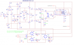
Greetings all! I was thinking that it would make sense that unwanted pulses on the output with a repetion frequency of 2 Hz has something to do with 555 timer, right? So I took out R131 and R232 (I am attaching again circuit diagram), each of them is connecting right (R131) and left channel (R232) to the 555. Now the pulses are gone and everything/both channels works as it should. If I put back R131, so only right channel is connected to 555, the amp still works. But, If I put back R232, I get unwanted pulses again. At first I thought that maybe 555 is not working properly, but then I should get unwanted pulses also when right channel is connected to it, right? Any ideas what should I look into it next? Thanks, any help and advice is much appreciated!
Attachments
You mean R231? ")
So it looks like the protection circuitry around T117 (T217 on the bad channel?) is kicking in. That transistor monitors the bias current and looks like it turns on if sufficient voltage is developed across the emitter resistors in the output stage.
See if there is sufficient B-E voltage to turn it on... if so then look at the bias current and emitter resistance values. If no voltage then possibly the transistor is faulty.
check out this replacement from Sanken:
https://www.semicon.sanken-ele.co.jp/sk_content/2sc2837_ds_en.pdf
https://www.semicon.sanken-ele.co.jp/sk_content/2sa1186_ds_en.pdf
because there are many counterfeits resp. fakes, I would only order there:
Transistors | Profusion.
BTW before replacement you must checking the reason for the defective output power devices. Otherwise, it could be that the new parts immediately fail again.
At best it is to prepair your amp in such kind, that it runs without the power output devices (only very small levels possible).
Only when the amplifier operates perfectly in this manner (include perfect DC measurements) you can mount the power transistors.
I haven't read all details, but I note, that there is no correct operation to observe after repair attempt. Obviously there wasn't perform my recommends from post #8.
After looking the schematic in post #28 I am able to mention all necessary steps.
Unusual is the fact, that the power follower triplet isn't in the NFB-loop, because the associated resistors R110/R111 are connected with the output of the VAS stage and not connected on the power output for the speaker (the only amp model I know, where this in this kind realized is Threshold's STASIS - go to first image of post #3 under
Threshold Stasis 3 Amplifier Capacitor Replacement
Most important thing is the correct operation of the front-end by it's own (only LTP and VAS stage).
To investigate this alone, follow steps are necessary (to perform at both channels for the aim of compare the measurements between the working and not working channel:
1) removing each power follower triplet T109-111-113 and T110-112-114 so as R120-121
2) From C, T106 to C, T108 two additional 8K-10K resistors in series and connection point (node) of both resistors to the power output
3) Connect R130 and R230 to GND (protecting mode isn't necessary here)
4) the NFB resistor - usually connected with the power output - must not be connected to the VAS output here, because this is already provided in the original topology - as mentioned above.
Next step: check out all voltage (and current) values arround the LTP and VAS stage.
according this schematic there must be follow values: T101-104 each 1-1,15 mA, T103 2-2,3 mA, T106-108 2-2,3 mA (Ube:300R)
Next step is the investigation of the variation range for the DC offset (turn arround the potentiometer between R103 and R106 from stop to stop (full range) and write down the two offset voltage values for both channels.
Now is to check the variation range of the BIAS voltage. Turn the potentiometer P for this purpose from minimum to the maximum.
The variation range should be approximately the same between both channels.
If this is the case, adjust the potentiometer to the lowest possible bias voltage to avoid thermal breakdown in the BjT power devices in later test steps
Only when all DC conditions are flawless at both channels, you can connect your speakers to the output for soundcheck without any risc of destroy. The undistorted volume level is extremely low, but loud enough to determine a proper operation during a long-term test.
After successful completion of this test, only the first two transistors of the power follower triplet are introduced again (T109-111 and T110-112) after carelully checking by transistor analyser.
The two additional 8K-10K resistors in series are now removed again from the speaker output. Instead this the resistor R119 is to replace with two 39R Resistors in serial mode (R119a and R119b) and connection point (node) of both resistors goes to the power output.
Now is to check again the variation range of the offset voltage and BIAS voltage over R119a/b.
Adjust again the potentiometer to the lowest possible bias voltage value
When all DC conditions are flawless again at both channels, you can connect again your speakers to the output for soundcheck. But please note, that the undistorted volume level is now a bit louder, but now there is the risc of a burned emitter resistor R119a/b. This means, that the listening level is to be kept very low during a long-term test.
After successful completion of this second test, the output devices are to connect, but only if the extra rectitier-capacitor unit DP1-4-C5/6 (only for the power output devices) so as the anti-plopp-/overcurrent protector unit with NE555 works in the right manner.
Connect now again R130 and R230 from GND to the previous connection place (PIN3 of NE555).
This URL's provides additional information:
YouTube
https://www.audiostereo.pl/topic/107052-densen-b100/
Oh, yes, I meant R231, thanks Mooly!
Tiefbassuebertr, thank you very much for this detailed instuctions! I have just found out that some of emitor resistors on the output stage of the left channel (the one that causes problems) were burned (I measured megaomhs instead of few ohms), so I replaced them and now both channels are working properly. Even more, the turn on thump is much lower now and there is almost no buzzing present in the right channel.
Still, if I will experience malfunction of the amp in the future, I will definetely take your steps as it will save me a lot of time. Thanks again!
I have another question, that is the value of bias current. I read here that someone use 50 mA for B-100. Although, here they suggest to go with the current of around 100 mA.
Is the value related only to the output transistors or whole output circuit topology?
And where to measure the voltage for calculation of bias current, is it ok if I measure it on R120 (I=U/R120) or shoud I measure on R120+R121, i.e. between emitors of output transistors (I=U/(R120+121))?
So the emitter resistors were open (some of them) which meant the volt drop across them would be higher than normal and tripping the protection.
Bias is determined largely by overall topology and would be around 130ma for this configuration and values, however thermal constraints (small heatsinks etc) might mean that value is not advisable. Go with the manufacturer recommended value, no higher. In practice, anything over a few milliamps will push crossover distortion way down.
Bias is determined largely by overall topology and would be around 130ma for this configuration and values, however thermal constraints (small heatsinks etc) might mean that value is not advisable. Go with the manufacturer recommended value, no higher. In practice, anything over a few milliamps will push crossover distortion way down.
Just to keep you updated, the amp has been working quite nicely for the last few weeks! I also added a DC block circuit by Rod Elliott and now I do not have any toroidal hum. I am still a bit annoyed by the turn on thump so I am thinking of adding also a soft start circuit...
Excellent 
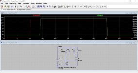
You won't beat a simple relay based speaker delay for eliminating thump. You can get these off the shelf or if you prefer, design your own.
Here's one I made earlier to save time later You can see the relay current in relation to the supply voltage. Simple circuits like this can easily be adapted to work of most supply voltages
You won't beat a simple relay based speaker delay for eliminating thump. You can get these off the shelf or if you prefer, design your own.
Here's one I made earlier to save time later
You can see the relay current in relation to the supply voltage. Simple circuits like this can easily be adapted to work of most supply voltagesAttachments
- Status
- This old topic is closed. If you want to reopen this topic, contact a moderator using the "Report Post" button.
- Home
- Amplifiers
- Solid State
- Replacement of output transistors in Densen B-100