No, turn on thump is related to poor design if it has always happened.
36 v out of 26.3 v winding is excellent.
You need to try the amp without speakers connected to see if the buzzing is coming from the transformer, or the speaker.
If coming from the transformer without speakers, check for mains DC with DC scale. Careful,use one hand only when probing socket; current across your heart can stop it. Wear no jewelry on hands wrists or neck, current or cap discharge through metal can burn your flesh to charcoal. If have significant DC on mains, shop for a line DC blocker as mentioned above. Make sure it is rated by agency like UL, VDE, etc.
If coming from the speaker, check the AC voltage on the filter cap powered up. Use one hand at a time and an alligator clip lead for the negative probe, AC voltage on filter cap should be no more than 200 mv or so. Most cheap meters do not have a function sensitive enough on AC to read this.
Another cause of speaker hum can be oxidized connections. Remove and replace connections power off to scrap any oxide off. This included pc board retaining screws with pads under them.
Other cause of speaker hum can be bad solder joints. I have this in my home built amp - silent friday, humming about 1/100 watt today. ****.
Last edited:
Thanks for suggestions! I will check if there is any DC on main and will go through possible oxidized connections. I will also borrow an oscilloscope and maybe this will give me some new insight. Will keep you all updated.
In respect to the turn on thump, did not expect such failed design from Densen...a bit disappointed.
In respect to the turn on thump, did not expect such failed design from Densen...a bit disappointed.
Update: I successfully replaced output transistors, I was able to get a combination of MJW3281A and MJW1302A. They work nicely and after first few listening tests it seems they are a very good substitute for original transistors. Thanks again for suggestions.
I still have the buzzing on the right channel. Today I got an oscilloscope and will try to find the source of the buzzing in the next few days.
I still have the buzzing on the right channel. Today I got an oscilloscope and will try to find the source of the buzzing in the next few days.
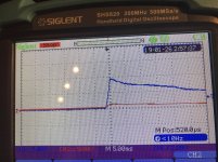
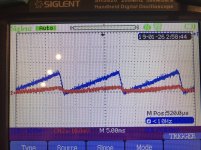
I did some initial basic measurements with an oscilloscope. Both measurements were done on amplifier output speaker sockets without speakers plugged in. On Figure 1 we have measurement of the turn on thump (blue - right channel, red - left channel). We can clearly see that there is a significant thump on the right channel that is also quite loud, left channel seems to be OK, I also do not hear anything on the left speaker. On Figure 2 we have the measurement of buzzing that can be heard on the right channel (oscilloscope is set here to a smaller amplitude range compared to Fig 1). Again, left channel performs better, there is a slight buzzing coming out of the left speaker but nothing significant. So, there must be something wrong with the right channel circuit, my guess would be that it has something to do with capacitors? I still need to check solder joints.
Attachments
Last edited:
I can't just see any (electrolytic) caps in the amp circuit itself aprt from one in the feedback return.
The 555 circuit seems shared between channels.
I would quickly check the DC conditions are the same for each channel. Low DC offset, similar bias currents and so on. Also check the front end currents are similar, easily done by looking at volt drops across the appropriate resistors.
I doubt there would be an issue but it just eliminates things.
The sawtooth is classic PSU ripple intruding on the audio, often caused by incorrect grounding.
Always remember amplifier circuits can not produce hum and buzz. It is there because it is being injected either into an input ground, or between two points of the circuit... such as those points sharing a common PCB trace with ripple current flowing in it.
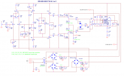
OK, i am having new problem and would like to ask for help on what to look. Suddenly I started to get 22 V of DC on the output of right channel. OK, I probably did something, but I have no idea what! I checked the voltage on collectors of both output transistor (T111 and T112 on included schematic) and they seem to be ok, that is +/- 35 V. But on emitters I have 23,5 V and 23,0 V. So I have collector-emitter voltage of around 12 V on one transistor and 58 V on the other! If it is in any help, I am including a schematic I found and this one is much more similar to the version of B-100 I have. Any ideas? Thanks in advance!
Attachments
Poking around with a probe might have burned something.
Usually DC offset is caused up in the front end or middle parts of the amp, including the drivers. Look for Vce on some transistor of zero, or Vbe of zero. Look for a capacitor with zero volts across it. Or a diode with 0 volts on it. The first stage with the unsymmetrical DC voltage is where you should concentrate your checks. Of course the feedback transistor T104 will show the offset on the output.
This is why I like to build & mess with single supply amps with a speaker capacitor. On direct coupled amps, you make one stupid mistake, or a soldering joint opens up, PFFFT there goes your speaker. My main speakers are $699 ea new.
With +- 35 v rails roughly, a couple of apex AX6 boards would fit in there nicely. They have the speaker cap. Advertised 50 W, I get 70 W for a second at a time out of mine. DC offset happens in an AX6, the sound gets funny when it gets loud. No expensive damage as long as the $3 output cap isn't too old & damaged. AX6 is single board so no interboard connections to oxidize & hum.
I came here from vacuum tubes, which were also nearly impossible to damage speakers with. If vacuum tubes oscillated ultrasonically, it damaged a $15 tweeter, not a $150 woofer.
Last edited:
You need to be sure you have the correct circuit, otherwise it all falls to pieces when we try to interpret results ")
There doesn't seem to be any global feedback on the diagram... do we take that at face value?
If you have plus 22 volts offset then you should be seeing that reflected in the reading at the base of T109 which would be around +24v give or take. You should also have around 650 millivolts across R114.
If you are sure the diagram is basically correct then do a copy of the circuit and write the voltages you measure at all the transistor nodes.
Thank you for your feeedback! It seems that the last version of circuit schematic I post is very much the same version of mine B-100 circuit, except the output transistors which are different in mine case since I already replaced them.
I first performed a measurement of Vbe on all transistors. Here I shouldn’t expect higher values than 0.7 V, right? I found out that Vbe is 8 V on T109 and T111. This is way too much and it probably means they’re faulty, right?
I first performed a measurement of Vbe on all transistors. Here I shouldn’t expect higher values than 0.7 V, right? I found out that Vbe is 8 V on T109 and T111. This is way too much and it probably means they’re faulty, right?
Well, yes, Vbe >1 v is a sign of a fault on silicon junction transistors.
Drivers and predrivers like TR109 & 111 are frequently taken out by the base current surging out of faulted output transistors. This often exceeds the Vceo rating. Why these would fail later after the output transistors were replaced is a bit of a mystery.
Drivers and predrivers like TR109 & 111 are frequently taken out by the base current surging out of faulted output transistors. This often exceeds the Vceo rating. Why these would fail later after the output transistors were replaced is a bit of a mystery.
Oh, they failed because I did something stupid while I adjusting bias, probably did short circuit with a probe or something similar. I hate myself for that, because before that everything worked!
OK, I will replace these two transistors and their complementaries, therefore I will need to find replacements. For T109 I have one, not so sure about T111, currently it'a D1763, probably will go with MJE15028/MJE15030.
As suggested, I also checked voltages on all diodes and capacitors, everything seems to be OK, no zero volts.
I first performed a measurement of Vbe on all transistors. Here I shouldn’t expect higher values than 0.7 V, right? I found out that Vbe is 8 V on T109 and T111. This is way too much and it probably means they’re faulty, right?
Well, yes and no
Forward biased and Vbe should always level out around 0.7 to 0.8 volts depending just how much current is flowing in the junction.
Reversed biased and its another story. The junction acts a little like a Zener diode and would give somewhere around 6 to 9 volts or so.
So polarity is all important. For the NPN's the base should be the most positive, for the PNP's the emitter will be the more positive.
get a 2200/35 cap and place it between speaker and amp while testing. positive to amp output
depending on transistor pinout, you could replace the to92 small transistors with PNP 2N5401 / KSA992 and NPN 2N5551 / KSC1845 (2N transistors have base as middle pin )
You could DIY a new amp eg LM3886 to one of Valery's ( VZaudio ) designs and place it where the old one was.
depending on transistor pinout, you could replace the to92 small transistors with PNP 2N5401 / KSA992 and NPN 2N5551 / KSC1845 (2N transistors have base as middle pin )
You could DIY a new amp eg LM3886 to one of Valery's ( VZaudio ) designs and place it where the old one was.
Last edited:
To mooly's point, forward biased silicon junction transistors should have Vbe less than a volt. The previous stage could cause a problem, and cause a transistor to be negative biased b-e. You have to observe the polarity of the transistor, npn or pnp, to know whether the part you are seeing is defective, or something ahead of it. npn have plus base, minus emitter, normally. pnp have the opposite. So something in the previous stage could cause an npn transistor to read -8v b-e.
If you are in North America I could suggest generic substitute transistors by package type, but distributor stocks in Europe & Asia are quite different, so I won't.
If you are in North America I could suggest generic substitute transistors by package type, but distributor stocks in Europe & Asia are quite different, so I won't.
Last edited:
OK, so I replaced transistors with too high Ube, npn T109 and also complementary pnp T110. I did the same for npn T111 and complementary pnp T112. Now I do not have a DC voltage on the output any more and correct Uce on the output transistors. BUT now I observe even stranger behaviour. See the image attached, this is what I captured on the output of the right channel. This pulse has a repetition frequency of exactly 2 Hz. But wait, It gets even stranger, its amplitude change with the resistor value of bias trimmer for the right channel while its duration changes with the trimmer value of bias for the LEFT channel?! I have no idea how this happened and I am on the verge of throwing everything out of the window. Do you maybe have any ideas?
I have no idea how this happened and I am on the verge of throwing everything out of the window. Do you maybe have any ideas?Attachments
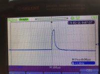
No ideas on that one tbh. Low frequency oscillation like that is not a logical fault... you would have to go back and check all the basics, perhaps measuring Vbe on the scope (don't connect the ground of the scope to anything other than circuit ground though).
Its an interesting problem though.
Did you confirm the polarity of the Vbe error before swapping parts because as I mentioned earlier, 8 volts isn't necessarily a fault if it is in a reverse bias state.
Its an interesting problem though.
Did you confirm the polarity of the Vbe error before swapping parts because as I mentioned earlier, 8 volts isn't necessarily a fault if it is in a reverse bias state.
The circuit may be beyond your capability to debug at this skill level. Your box, transformer, rectifiers, filter caps, controls, heat sinks are useful. Two LM3886 kit boards would probably fit in there nicely. Couldn't begin to recommend a vendor without knowing the continent you are on.
I just put away a LM1875 project that was resolutely motorboating like that. Concluded the IC was incompatible with point to point wiring. Boards available on e-bay for LM1875 are dedicated speaker burners,& require a center tap transformer I don't have.
Instead I bought a blown PA amp (PV-4c) for $38 with freight, put $35 of new parts in it (4 output transistors & pads,4 filter caps,2 input caps, more heat sink), listening to it right now. Clean safe sound. Has DC on speaker detect and crowbar circuit that blows the breaker.
Last edited:
- Status
- This old topic is closed. If you want to reopen this topic, contact a moderator using the "Report Post" button.
- Home
- Amplifiers
- Solid State
- Replacement of output transistors in Densen B-100