So, the feedback resistor in a CFA is often (very) low, not because the feedback node needs 'a lot' of current, but because of stability considerations.
And where does all that current go then, that flows into the low value feedback resistor? To ground, of course, through the shunt R.
Jan
And where does all that current go then, that flows into the low value feedback resistor? To ground, of course, through the shunt R.
Jan
More because of needed loopgain than only stability. It is a key for understanding of the CFA function that loopgain is Zt/Rf and does not depend on Rf/R1, where R1is from FB node to ground. And also because of low -Zin value the FB divider impedance is to be low. All composed together. Zt is a kind of equivalent to Ao of the VFA.
That's a decent approximation. Accounting for the (-) input impedance Ri, the voltage loop gain at the output (see next paragraph) is very close to ( Rg / (Rg + Rf')) * Zt / ( Rf' || Rg + Ro ), where Rf' = Rf + Ro, and Ro is the open loop output impedance. If Ri and Ro are taken as zero, this is identical to the approximation.
From above reference, we have to be careful when we talk about loop gain. Middlebrook points out that voltage and current loop gains generally vary depending on where in the circuit they are measured, although the total loop gain (taking both into account) is insensitive to measurement location.
From above reference, we have to be careful when we talk about loop gain. Middlebrook points out that voltage and current loop gains generally vary depending on where in the circuit they are measured, although the total loop gain (taking both into account) is insensitive to measurement location.
Hello DPH. Yes, good discussion!
Just for reference/discussion, I am using 1k feedback R in a 240 Watt amp and 540 ohms in a 100 Watt. The shunt to ground is 22 ohms in the latter and 33 in the former.
The peak feedback current into the TIS is 8x the standing current (1 mA). I use a very fast rise time signal to check this. BTW, diamond buffer still remains in class A - this requires some input bandwidth limiting and judicious selection of Rf.
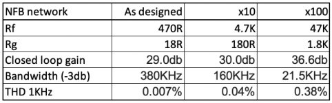
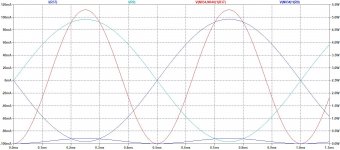
I ran a few quick and dirty simulations on one of my CFA designs.
Here is what we see (attached). All options are shown for the same output swing (20V RMS @ 8 ohm). I keep the Rf/Rg ratio the same.
The results pretty much confirm the considerations mentioned above (Jan, Pawel, CPaul). Higher feedback network values lead to narrower bandwidth, higher CLG (lower loop gain), resulting in higher distortion.
I was wrong with the assumption the low impedance "-" node requires the low impedance feedback network for controlling it - actual reasons for the low impedance FB network are explained in the posts above.
Thank you guys for the good discussion.
Cheers,
Valery
Attachments
I ran a few quick and dirty simulations on one of my CFA designs.
Here is what we see (attached). All options are shown for the same output swing (20V RMS @ 8 ohm). I keep the Rf/Rg ratio the same.
The results pretty much confirm the considerations mentioned above (Jan, Pawel, CPaul). Higher feedback network values lead to narrower bandwidth, higher CLG (lower loop gain), resulting in higher distortion.
I was wrong with the assumption the low impedance "-" node requires the low impedance feedback network for controlling it - actual reasons for the low impedance FB network are explained in the posts above.
Thank you guys for the good discussion.
Cheers,
Valery
Did you change the compensation too ?
Another view.I was wrong with the assumption the low impedance "-" node requires the low impedance feedback network for controlling it - actual reasons for the low impedance FB network are explained in the posts above.
Take, to simplify, a so-called CFA (sorry, for the so-called, I can't agree with the CFA naming) using a single transistor input stage.
When the feedback network is not connected to the output stage, the load seen by the emitter of the input transistor is only that of the bottom resistor of the feedback network which usually is of a low value, 100 to 1000 Ohm typically.
When the feedback is connected to the output stage, the AC current through the bottom resistor is highly increased, so the emitter sees a much higher impedance. The whole functionning is mainly under the control of the base emitter voltage (Vbe) of the input transistor.
It reminds me the operation of Sziklai pairs, bootstrapped or current dumping circuits where an AC current, synchronised with the input signal through feedback, enhances the impedance of the load seen by their output.
In CFAs, the inverting input can be considered as a local output which is not the case in a VFA where the inverting input has a very high impedance and does not deliver current.
Last edited:
Did you change the compensation too ?
Yes, I changed the lead compensation cap value in roughly the same proportion.
Another view.
Take, to simplify, a so-called CFA (sorry, for the so-called, I can't agree with the CFA naming) using a single transistor input stage.
When the feedback network is not connected to the output stage, the load seen by the emitter of the input transistor is only that of the bottom resistor of the feedback network which usually is of a low value, 100 to 1000 Ohm typically.
When the feedback is connected to the output stage, the AC current through the bottom resistor is highly increased, so the emitter sees a much higher impedance. The whole functionning is mainly under the control of the base emitter voltage (Vbe) of the input transistor.
It reminds me the operation of Sziklai pairs, bootstrapped or current dumping circuits where an AC current, synchronised with the input signal through feedback, enhances the impedance of the load seen by their output.
In CFAs, the inverting input can be considered as a local output which is not the case in a VFA where the inverting input has a very high impedance and does not deliver current.
A CFA and a Sziklai pair are indeed quite similar. I remember a paper where this was further discussed. I'll see if I can find it.
Jan
Last edited:
Take, to simplify, a so-called CFA (sorry, for the so-called, I can't agree with the CFA naming) using a single transistor input stage.
The Thevenin equivalent of the output, Rf and Rg is a voltage source in series with a single resistor R. Virtually all of the signal current in the transistor's collector comes from the scaled output through resistor R; signal current fed from the scaled output is the input stage's signal output. So why the objection to the term CFA to describe what is happening here? (In a VFA, virtually none of the collector current comes from the amplifier's output; it is steered from an input stage source by the inputs' differential voltage. Hence, a VFA.)
Last edited:
It might be that not everyone likes the CFA naming convention, but it does not change the fact that the -ve input on a CFA is a current input port and the output of the diamond buffer (on the associated transistor collectors) a current.
Nice article in AudioXpress BTW Chris!
Nice article in AudioXpress BTW Chris!
Another view.
Take, to simplify, a so-called CFA (sorry, for the so-called, I can't agree with the CFA naming) using a single transistor input stage.
When the feedback network is not connected to the output stage, the load seen by the emitter of the input transistor is only that of the bottom resistor of the feedback network which usually is of a low value, 100 to 1000 Ohm typically.
When the feedback is connected to the output stage, the AC current through the bottom resistor is highly increased, so the emitter sees a much higher impedance. The whole functionning is mainly under the control of the base emitter voltage (Vbe) of the input transistor.
It reminds me the operation of Sziklai pairs, bootstrapped or current dumping circuits where an AC current, synchronised with the input signal through feedback, enhances the impedance of the load seen by their output.
In CFAs, the inverting input can be considered as a local output which is not the case in a VFA where the inverting input has a very high impedance and does not deliver current.
That's exactly the point that made me confused at some point
The "-" input node is "bootstrapped" by the input signal, so its effective impedance is higher than it would be if the base would be static.
Hi Ian,A CFA and a Sziklai pair are indeed quite similar. I remember a paper where this was further discussed. I'll see if I can find it.
Jan
Is the paper Ed Cherry's ‘Feedback amplifier configurations’, IEE Proceedings on Circuits, Devices and Systems, Vol 147, No 6, Dec 2000 ?
You quoted Cherry's CFA bit here Is it possible to create any active circuit with zero feedback?. The full article is available here.
I posted on the CFA being essentially a CFP here Current Feedback Amplifiers, not only a semantic problem? (which links to here).
Bob Cordell has posted several times the similarity of the CFA to the RIAA two transistor stage, as well as to the CFP recently, but can't find it right now (maybe someone can help).
Cheers
It is understandable that some would object on an historical basis to the application of the term CFA to a certain type of amplifier by the semiconductor industry. Understandable, that is, if it is acknowledged that this practice is nevertheless technically accurate. After all, the circuit feeds a current from its output back to, and even through, its input stage. Hence, it’s a current feedback amplifier.
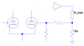
Ironically, this situation is precisely reversed in the case of some circuits which have been with us for quite a while.
The attached schematic’s “current feedback amplifier” routes its load's current through resistor Rs, giving rise to a voltage. Some portion of this voltage is applied to the inverting input of a gain block, whose topology is clearly that of a VFA. There is absolutely no feedback of current here. This is simply a VFA controlled by a voltage which is proportional to its load’s current.
Conscientious objectors of both stripes can choose to dig in their heels, play the parts of iconoclastic curmudgeons, and refuse to use the acronym CFA as the rest of the world does. Or they can put double quotes around it (guilty as charged in this post) as they deem appropriate. Or maybe even write 'CFA (sic).' But what’s the point? Is there any hope that the rest of humanity will change its behavior?
Better in my mind for all of us to grit our teeth and use the word as everyone else does, while always being aware of the context.
Attachments
- Home
- Amplifiers
- Solid State
- Current Feedback Amplifiers, not only a semantic problem?