Nataly eXPerience. Without compromise.
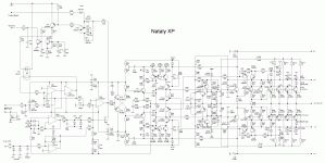
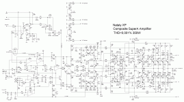
This is the last in the series of my amplifiers "Nataly" development today. It used all the useful insights that were used in previous versions and takes into account the nuances of correction. Used SuperA mode output stage, which can significantly reduce the distortion of higher order. The amplifier is equipped with a limiter, protection of the output stage, the signal compensation on the speaker wires.
The first stage of the amplifier performs the function of the doubling of the input voltage, and a peak limiter. The output of the operational amplifier is loaded on the buffer stage, preserving the work of the Operational Amplifier in class A.Main stage is inverting composite amplifier. Such a construction eliminates the common-mode voltage at the inputs of the Operational amplifier. In the summing point also receives the correction signals zero amplifier output from the integrator, double inverted voltage drop on the "ground" speaker wire for the virtual removal of the speaker wires from the system. The voltage amplifier has a gain of 5.1 kω\470 Ohm ) +1, it is protected from overload by output current when the protection operation.
The BIAS source is controlled dynamically, the control circuit the quiescent current support output transistors in active mode.
Peak limiter monitors emerging at the time limitation of output signal output voltage output OP4, decreases the gain of the first stage (OP1) and served a light signal to the user.
Attachments
Last edited:
Let's started!
Please use online translator from russian for reading.
Nataly Experience - ???????? ????????? - ????? ?? ????????????????
Please use online translator from russian for reading.
Nataly Experience - ???????? ????????? - ????? ?? ????????????????
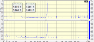
Because Assembly into the finished design is not yet completed, measurements are premature . But expect about 0.0005% of and less of.
Interesting. Another amp inspired by Eric Margan's idea.
See also Linear Audio | your tech audio resource
See also Linear Audio | your tech audio resource
It was one of many ideas used in this amplifier, but it has been significantly improved to work well in a real environment and it does not burden the stages of the amplifier voltage.
Yes, it is my design.
Complete electrical isolation of the control circuitry from the signal.
But because of the variation in specific optocouplers reproducibility of the results was not very good, had to do an exact fit.
Complete electrical isolation of the control circuitry from the signal.
But because of the variation in specific optocouplers reproducibility of the results was not very good, had to do an exact fit.
Final of works. Stable and optimised scheme/PCB.😎
Attachments

Last edited:
looks interesting i love complex designs it's usually sounds great .... what about your test results ?
While it was not measured as it is not ready the final form factor, but considering that the earlier version V.2012 PRO was shown less 0,0008% at 10kHz...😉
Consider:
1) greatest feedback depth (at 6dB)
2) SuperA mode vs. AB class on out stage.
3) Current mirror+caskod in voltage amplifier stage vs common emitter inclusion.
4) OPA827 vs AD825
Well identified and provisions for correction, allowing, in particular:
A) a complete rejection of the correction over Miller in the voltage amplifier stage.
B) reduce the load on the voltage amplifier stage (instead of 2*100 pF, you can leave 2* (68...82 pF)
C) Decrease correction ahead with 100pF to 56pF.
D) Reducing correction ahead on OpAMP OP4 through C19 from 10 to 5.1 pF.
Place your bets, gentlemen! 🙂
Last edited:
signal to noise ratio of the amplifier?
What are the parameters of the amplifier signal to noise ratio of the amplifier?
What are the parameters of the amplifier signal to noise ratio of the amplifier?
For amplifiers, this parameter is large does not make sense because the noise is less self-noise, for example, the oscilloscope at the limit of measurement 1 millivolt per division.
No, double-sided PCB only. Tracing is very important for low THD level.
No changes in correction were made - default capacitors nominals. With the further decrease of the correction parameters are expected to be even more interesting.
No changes in correction were made - default capacitors nominals. With the further decrease of the correction parameters are expected to be even more interesting.
Last edited:
EMU 0404USB with all "surprises", such as a higher distortion level at left channel. Therefore, the measurements were carried out in the right channel, respectively, the distortion of the amplifier is displayed on the chart right channel.
Interesting - what were the test parameters ? Output power / amplitude /load ?
While it was not measured as it is not ready the final form factor, but considering that the earlier version V.2012 PRO was shown less 0,0008% at 10kHz...😉
Consider:
1) greatest feedback depth (at 6dB)
2) SuperA mode vs. AB class on out stage.
Could you explain what is SuperA mode?
3) Current mirror+caskod in voltage amplifier stage vs common emitter inclusion.
4) OPA827 vs AD825
Well identified and provisions for correction, allowing, in particular:
A) a complete rejection of the correction over Miller in the voltage amplifier stage.
What is rejection of the correction? Could you explain that?
B) reduce the load on the voltage amplifier stage (instead of 2*100 pF, you can leave 2* (68...82 pF)
C) Decrease correction ahead with 100pF to 56pF.
Again I don't understand, decrease correction, what you mean by that?
D) Reducing correction ahead on OpAMP OP4 through C19 from 10 to 5.1 pF.
Again the same??
Place your bets, gentlemen! 🙂
The circuit looks very interesting, but your explanation how it works is very strange and cryptic.
SuperA mode - is a non-switching mode for output and drivers stage (JVC patent). For BIAS current is the same as AB mode, but dynamically adds current for prevention of close non-active transistors.
Full deletion of C34,C36 or decrease them to 5,1...10pFWhat is rejection of the correction? Could you explain that?
it was about C45, C46 and C32,C33.Again I don't understand, decrease correction, what you mean by that?
no same, it is OpAmp local forward correction.D) Reducing correction ahead on OpAMP OP4 through C19 from 10 to 5.1 pF.
Again the same??
- Status
- Not open for further replies.
- Home
- Amplifiers
- Solid State
- Nataly eXPerience