Hi:
Is there any particular stage or function within an amplifier where low gain (low beta or hFE) transistors are preferable to high gain?
Is there any particular stage or function within an amplifier where low gain (low beta or hFE) transistors are preferable to high gain?
Corrolary
Is it ever preferable to *not* choose the highest gain version of a transistor that is offered as several models of varying gain, for ex: 2SC|KSC3503[D|E|F] ?
Is it ever preferable to *not* choose the highest gain version of a transistor that is offered as several models of varying gain, for ex: 2SC|KSC3503[D|E|F] ?
Many: when you need the highest voltage gain or the best linearity are the first that come to mind, but if you think more deeply, there must be many others.Hi:
Is there any particular stage or function within an amplifier where low gain (low beta or hFE) transistors are preferable to high gain?
Why do you think manufacturers care to sort and mark "A" groups (for european types), when they could simply leave them without suffix? (they too exist).
Everything is a matter of tradeoffs, and semiconductor engineering is no exception: when you favor some parameter, a few other ones follow mechanically, while most of others go in the opposite (unwanted) direction.
The β factor has a big advantage for the average sucker: it is just a simple scalar figure, easy to memorize and compare. Nothing to get a headache from, and the certitude to get "the best" for a given amount of money....
in a Darlington configuration is the best place.
For the driver or the driven element of the pair?
More importantly: Why, if the point of a Darlington pair is to gain as much gain as possible?
for DIY no
for product development, yes finding suitable replacements in long term production run and support, after Vendor X decides to not offer that high grade part anymore maybe stuck in a dead end.
design for widest range, means pick circuits that work within reasonable minimum gains aren't sensitive to wide variations either.
why?
For the driver or the driven element of the pair?
More importantly: Why, if the point of a Darlington pair is to gain as much gain as possible?
sorry that was a bad joke, I reckon that what semi house's do with their "dogs" on the pass device.
Many: when you need the highest voltage gain or the best linearity are the first that come to mind, but if you think more deeply, there must be many others.
Ok, I can understand the possibility that if there are two parts (A vs. B) and A has hFE varying from 50-200 whereas B has 40-60, then B could be preferable since it may yield better linearity.
I don't get why lower hFE would lead to higher voltage gain?
At my present level of understanding, I've derived the small signal T model. My implementation has a collector current source: ic=gm*vbe, with gm=Vt/Ic. The intrinsic emitter resistance is: re=(1/gm)*hfe/(hfe+1), with hfe=hFE(Ic).
In a sense, the emitter resistance (as given by re=Vt/Ic) is "adjusted" to account for the fact that some base current flows.
Based on your comment, at first I thought this might affect voltage gain, but no, it doesn't. At least for CE, it seems to me that voltage gain is determined only by gm and the load impedance.
Care to elaborate further? Thanks!
sorry that was a bad joke, I reckon that what semi house's do with their "dogs" on the pass device.
Oh, I get it. :-D
I think hes saying that graded devices have many other parameters that are affected by semi processes and its a bit simplistic picking one parameter like current gain when you might interested in Vceo which might be in reality inversely related.
Last edited:
The completely linear small signal model is not helpful in understanding non-linear phenomenons, by definition.Ok, I can understand the possibility that if there are two parts (A vs. B) and A has hFE varying from 50-200 whereas B has 40-60, then B could be preferable since it may yield better linearity.
I don't get why lower hFE would lead to higher voltage gain?
At my present level of understanding, I've derived the small signal T model. My implementation has a collector current source: ic=gm*vbe, with gm=Vt/Ic. The intrinsic emitter resistance is: re=(1/gm)*hfe/(hfe+1), with hfe=hFE(Ic).
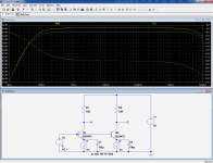
However, even the linearized small-signal model is already sufficient to show some things, see below.
You have to remember that all semiconductors parameters are correlated in some way, which is why relying on a single one such as β can be seriously misleading
Attachments
- Status
- Not open for further replies.
- Home
- Amplifiers
- Solid State
- Is it ever desirable to have *low gain* transistors?