can i use k177-gr or k170-bl ? Any change needed ?
Hi Didiet,
You can use k170 (both gr and bl). Optimal source degeneration resistors (R32, R54) value for jFETs will be 220R (actually, same for k117). Drain current is stabilized at 1.54mA per shoulder here.
k170 is a little bit slower than k117, but also a bit lower-noise one, however in this particular case you will most likely not notice the difference (because of the high GNFB loop gain in this design). In terms of SOA - also no problem.
Cheers,
Valery
So i will fine with > 2ma Idds ?
Any updated schematic ?
I'm trying to make pcb for FetSuMo, and find you layout have servo. Which component i need to change for 35-45V supply ?
Thanks.
Any updated schematic ?
I'm trying to make pcb for FetSuMo, and find you layout have servo. Which component i need to change for 35-45V supply ?
Thanks.
Member
Joined 2009
Paid Member
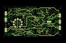
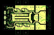
Developed the layout for IPS section. 3"x5.7" double layer.
That's a nice looking pcb layout. I am thinking the same as you for my own hybrid - provide footprints for SS IPS just in case. But I do like to see a tube in there

But I do like to see a tube in there

I did some comparisons.
Although the tube gives the lowest gain, comparing to jfet and bjt at the input, it provides the best linearity, maintaining very low noise (as I can see in my earlier prototypes), and glowing in the dark.
Excellent, hard to beat combination! 😛
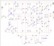
+/-40V supply k170 option
Hi Didiet,
Idss shows the value of drain current at zero g-s offset. In our case, the drain current is set by CCS at 1.54 mA per jfet, which is fine for both k170 and k117 at any rating (gr and bl), g-s offset will setup automatically (the circuit is self-balancing).
Despite the fact I use DC servo, I have left the trim-pot between jfet sources - it will be possible to micro-trim for the lowest distortion (although it will be low enough even with no trimming).
Here is the schematic, adjusted for +/-40V supply, this one will work fine in +/-35V to +/-45V range of supply voltages, giving more or less 50W at 8 ohm output power. In fact, in this case you can use just one pair of output FETs - more than enough for this power level (even for 100W at 4 ohm).
Use the small local heatsinks for U3, U4 (around 0.35W dissipation here).
Cheers,
Valery
P.S. You can also add some more electrolytics to the power rails - I omit them for sim purposes (they slow-down the model as it runs at 1/10-th of the real time).
So i will fine with > 2ma Idds ?
Any updated schematic ?
I'm trying to make pcb for FetSuMo, and find you layout have servo. Which component i need to change for 35-45V supply ?
Thanks.
Hi Didiet,
Idss shows the value of drain current at zero g-s offset. In our case, the drain current is set by CCS at 1.54 mA per jfet, which is fine for both k170 and k117 at any rating (gr and bl), g-s offset will setup automatically (the circuit is self-balancing).
Despite the fact I use DC servo, I have left the trim-pot between jfet sources - it will be possible to micro-trim for the lowest distortion (although it will be low enough even with no trimming).
Here is the schematic, adjusted for +/-40V supply, this one will work fine in +/-35V to +/-45V range of supply voltages, giving more or less 50W at 8 ohm output power. In fact, in this case you can use just one pair of output FETs - more than enough for this power level (even for 100W at 4 ohm).
Use the small local heatsinks for U3, U4 (around 0.35W dissipation here).
Cheers,
Valery
P.S. You can also add some more electrolytics to the power rails - I omit them for sim purposes (they slow-down the model as it runs at 1/10-th of the real time).
Attachments
Last edited:
vzaichenko
What a nice VAS stage !! I must be blind that didnt spoted it before.
Looks really promising. Looking fore further updates.
thx
What a nice VAS stage !! I must be blind that didnt spoted it before.
Looks really promising. Looking fore further updates.
thx
Hi Didiet,
Idss shows the value of drain current at zero g-s offset. In our case, the drain current is set by CCS at 1.54 mA per jfet, which is fine for both k170 and k117 at any rating (gr and bl), g-s offset will setup automatically (the circuit is self-balancing).
Despite the fact I use DC servo, I have left the trim-pot between jfet sources - it will be possible to micro-trim for the lowest distortion (although it will be low enough even with no trimming).
Here is the schematic, adjusted for +/-40V supply, this one will work fine in +/-35V to +/-45V range of supply voltages, giving more or less 50W at 8 ohm output power. In fact, in this case you can use just one pair of output FETs - more than enough for this power level (even for 100W at 4 ohm).
Use the small local heatsinks for U3, U4 (around 0.35W dissipation here).
Cheers,
Valery
P.S. You can also add some more electrolytics to the power rails - I omit them for sim purposes (they slow-down the model as it runs at 1/10-th of the real time).
Valery, I have a few question about this amp.
1. Why you use so low current for 2SK170, jfet works best with drain current close to its Idss?
2. Why so high jfet degeneration, it is waste of gain?
3. Why use of blue LED to bias cascade, the bleu LED has highest noise?
4. Why you use shun resistors (R23, R24) in the VAS to lower the gain? Is it not better to use it (the gain) in NFB, locally perhaps?
5. I suggest you to use bjt bias spreader instead simple resistor, lower impedance, and you don't put it on the heathsink of course.
6. I think that you use to low degeneration in bjt LTPs.
Just mine opinion, Damir
PS. You use low resolution spice, it's time to switch to LTspice, and then you can share the .asc files as most people here use LTspice.
Last edited:
Hi Damir! My answers are inline below:
1. Why you use so low current for 2SK170, jfet works best with drain current close to its Idss?
*** In many cases, higher drain current = higher noise. 3mA tail current is a sort of a practical optimum (based on experience). Also, my initial thinking was 2SK117, for 2SK170 quiescent current may be set slightly higher (4-4.5mA at the tail?).
2. Why so high jfet degeneration, it is waste of gain?
*** OLG of this design is very high - with low degeneration you will have 120db easily, maybe even more. In such situation, it's better to use some of it for local NFB (which degeneration is), ensuring better linearity and frequency response of particular cascade (LTP in this case).
With regards to GNFB loop gain, "the more is the better" is not the right approach. If you want smooth transients handling, you need to keep each stage's OLG under control.
Experiments with my earlier hybrid showed the best results with the following gain distribution:
1-st LTP 10.8 db
2-nd LTP 18.7 db
VAS 45.7 db
Overall OLG 75.3 db
CLG 28.5 db
LG 46.8 db
So, I don't want to have the first LTP OLG higher than, say, 12db.
3. Why use of blue LED to bias cascade, the bleu LED has highest noise?
*** This is a good point - I will a slot for the 2-nd LED on each side, so that I will test the live prototype with the blue ones and with a pair of red ones. Slightly higher offset, but never mind - it will be very interesting to see what practical difference noise-wise will be observed.
4. Why you use shun resistors (R23, R24) in the VAS to lower the gain? Is it not better to use it (the gain) in NFB, locally perhaps?
*** Also a good question. I tested this kind of shunt load for VAS with different OPS topologies some time ago. When you have a "complex", non-linear, input impedance of your OPS - this is what you have in many cases and this is what we have here, loading VAS with a constant resistive load helps to "mitigate" this non-linearity. In this particular case, the shunt us rather high R, I saw designs (well performing!), where VAS was loaded with 7.5K. Exactly for the purpose I just mentioned.
Again, we've got a bunch of excessive gain to spend here 😉
5. I suggest you to use bjt bias spreader instead simple resistor, lower impedance, and you don't put it on the heathsink of course.
*** Possible option, again - worth practical testing. Resistor is low here, so - should not be a problem. But I will try a simple spreader as an experiment.
6. I think that you use to low degeneration in bjt LTPs.
*** This pair of LTPs doesn't need to be too much balanced individually (unlike the first LTP), so... again a question - how much gain I'd like to drop here. rather difficult to understand from the simulation, so I will make some tests on the prototype. But the point is good - maybe a bit higher degeneration will allow balancing them between each-other. Need to see the real spectrum to understand if this is really the case.
Thank you for the questions - made me think once again about some things... which is always good 😉
Cheers,
Valery
Hi vzaichenko,can you share fetsumo and bjtsumo multisim file?
Hi Caglarm, I can send them to your e-mail for your personal use - please let me know the address.
Cheers,
Valery

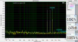
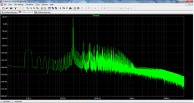
Not bad 😉 Low IMD is pretty much expected here... though those "products" on the right are rather "dense". Well somewhere close to -100db, but still - interesting where they come from.
Did you try to compare with jfet version? As well as with the tube one? Just curious.
Have you got 12AU7 model by any chance?
Did you try to compare with jfet version? As well as with the tube one? Just curious.
Have you got 12AU7 model by any chance?
Not bad 😉 Low IMD is pretty much expected here... though those "products" on the right are rather "dense". Well somewhere close to -100db, but still - interesting where they come from.
Did you try to compare with jfet version? As well as with the tube one? Just curious.
Have you got 12AU7 model by any chance?
I have download many tube model for LTspice, but still didn't use them 😀
I will try jfet version. But I have to sleep again....zzzzzz.....
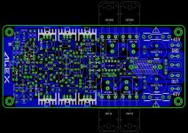
..... and PCB with one layer , not finished yet .....😉
Regards ,Alex
That was very quick

- Home
- Amplifiers
- Solid State
- Ultra-high performance, yet rather simple - hybrid and more!