The common emtter/collector/base amplifier stage consists of one amplifying device
I'm sure you can see some similarity between the common emitter amplifier and the CFP on the positive rail on that schematic.
That CFP does not have gain, it does not increase much the transconductance of the compound stage in relation to a single transistor, afaik. This is because Re=Rc=100 ohms on the pnp bjt. It only inverts the phase, and the feedback to the emitter of the npn makes that node behave as a collector.
rather than balanced to ground.
Inventing new meaningless statements to cover up a misunderstanding is like digging deeper in an effort to get out of a hole.

Jan
I didn't think there was an example of this using BJTs; turns out there is, and more than one. I'm referring to the amplifiers by Musical Fidelity, designed by the late Tim de Paravicini. He used common-source and common-emitter outputs. The one that I'm attaching uses BJTs in quasi-complementary topology (but the CFP is on the positive rail to make a common emitter).
Spice says:
It's a pseudo non switching "class A" and each LTP controls the voltage on one side of the output, on the transistor side of the emitter resistors, not on the output side. So it's very good as long as you don't run out of bias, but the transition out of class A and into class-AB really sucks, because one LTP drops the ball when its transistor stops conducting.


With enough bias it should sound good though.
The common emtter/collector/base amplifier stage
What (the hell) is memory distortion? What causes memory distortion? How can memory distortion be "canceled"?
As I wrote earlier memory distortion is a misleading phrase.
It is not the memory that is distorted. Due to the effect the distortion will have a memory. The distortion will depend on the state of the amplifier 1 to 100 milliseconds before or even on what happened to the smaller transistors within the previous half-period.
Mainly the exponential heating and cooling behavior of solid state devices causing that type of distortion.
Measurement example that a simple BJT has thermal memory. Circuit not needed for thermal distortion generation. It's inherent in solid state devices:
https://www.diyaudio.com/forums/solid-state/5928-comments-thermal-distortion-2.html#post6339797
So the goal is to minimize the memory of the amplifier. High memory -> bad sound. Low memory -> good sound.
Measurement example of High memory low THD BJT amplifier [1mV/div], Low mermory high THD tube amplifier [2mV/div] and Very low memory very low THD BJT amplifier [0.05mV/div] here:
https://www.diyaudio.com/forums/solid-state/5928-comments-thermal-distortion-2.html#post6339800
Even the tube fanatics loved the latest amp based on the audition.
Jan Didden attached an error vs. time diagram from Dr. Kolinummi in post #70. <- That is the memory (type) distortion!
Do you see now that the distortion has a memory?
Inventing new meaningless statements to cover up a misunderstanding is like digging deeper in an effort to get out of a hole.
You don`t understand the purport of the well established topological classification "single ended" and "balanced".
Do you see now that the distortion has a memory?
No. Obscurity remains.
Thermal distortion and memory distortion have a different origin.
Memory distortion ought to refer to remanence (remanent magnetization, magnetic memory) that afflicts both ferromagnetism and paramagnetism. The subject has been explored in great detail, your chances of coming up with something of value using stupid sofware simulations is equal to zero.
The presence of thermally excited charges is a source of distortion while remanent magnetization decays at a faster rate with increasing temperature.
A faster polarization does not imply higher polarizability or a more consistent polarization, likewise a faster depolarization does not imply less remanence. On the contrary, the polarization / depolarization anomalies are closely related to saturation and high transition velocity. Also, a slow depolarization process by which heat is essentially generated is necessary for a healthy signal development.
Now, what is your method of reducing thermal distortion and memory distortion?
You don`t understand the purport of the well established topological classification "single ended" and "balanced".
Well, I've been asking for explanations of posts of you I didn't get, repeatedly, but these were never forthcoming.
The inescapable conclusion is you don't know yourself and are just throwing up random statements.
Disappointing.
Jan
Last edited:
Since the common emitter/collector/base amplifier by definition consists of one amplifying device, its input and output necessarily have to be referred to ground by a passive component.
An amplifier stage comprising two amplifying devices in series connection, the input and output necessarily have to be balanced to ground. The result is markedly altered transfer characteristics:
Markedly raised amplification factor / efficiency
Markedly raised instability
Markedly raised distortion
Markedly distinct spectral content
I have not made up anything.
The common emitter/collector/base amplifier stage consists of one amplifying device where the common input/output terminals are referred to ground rather than balanced to ground.
I'd like to understand what you mean by this. "referred to ground rather than balanced to ground"?
Jan
Anyway...
As I understand it, Thermal Memory in solid state devices is produced by current passing through the junctions, generating increase in temperature of said junctions, which last for a certain time (a "temperature tail"), which causes a transitory change in the amplifying properties of the device and which is not in sync with the complex musical signal. Hence distortion occurs...
The proposed remedy from the Wise is: keep power as constant as possible in the significant device...and I would add, as low as possible...
(Maybe not entirelly correct explanation but you know what I mean).
I propose another circuit to play with the hypothesis, or simply replace your input pair with a bootstrapped CFP in a daughter-board.
The LSK170 being easier to find than the P channel.
Edit: though VFETs are best at the output, this one with Mosfets is also cool, easier to find and way cheaper.
Cheers,
M.
Attachments
Last edited:
Another unusual circuit
Good explanation dear Mauricio. Unlike tubes, solid state semiconductors suffer a big change of parameters with change of temperature. Feedback might fail to correct this, as Pierre has shown: Memory Distortion Philosophies
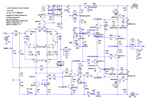
Back to "unusual circuits"... Altough I really dislike the brand name, I have to show this one. It is a preamp, single ended out (common source again), cascoded. Uses lateral mosfets, TO220 driver type: 2SJ77 2SK214. Using medium power TO220 and using cascodes helps with the memory type distortion.
The unusual thing is T11 and T15, at the output stage, with gates connected to the drains. The only explanation provided is "it reduces crossover distortion" (T11 and T15). But how? I think it's due to the capacitances of the complementary devices: when current has to change through cascode T10, the charge on the device capacitances must change, and these capacitances create an error at high frequencies as we know. The higher the frequency the higher the distortion due to the capacitances. But the complementary device T11 partially cancels this error, because the charge at its capacitances must change by a similar amount in opposite polarity. Same for cascode T20 and "correction" T15. The cancellation will be partial because they are not perfect complements. It's a similar situation to a fully complementary diff pair with jfets (John Curl): there is partial cancellation of the gate capacitances.
Good explanation dear Mauricio. Unlike tubes, solid state semiconductors suffer a big change of parameters with change of temperature. Feedback might fail to correct this, as Pierre has shown: Memory Distortion Philosophies
Back to "unusual circuits"... Altough I really dislike the brand name, I have to show this one. It is a preamp, single ended out (common source again), cascoded. Uses lateral mosfets, TO220 driver type: 2SJ77 2SK214. Using medium power TO220 and using cascodes helps with the memory type distortion.
The unusual thing is T11 and T15, at the output stage, with gates connected to the drains. The only explanation provided is "it reduces crossover distortion" (T11 and T15). But how? I think it's due to the capacitances of the complementary devices: when current has to change through cascode T10, the charge on the device capacitances must change, and these capacitances create an error at high frequencies as we know. The higher the frequency the higher the distortion due to the capacitances. But the complementary device T11 partially cancels this error, because the charge at its capacitances must change by a similar amount in opposite polarity. Same for cascode T20 and "correction" T15. The cancellation will be partial because they are not perfect complements. It's a similar situation to a fully complementary diff pair with jfets (John Curl): there is partial cancellation of the gate capacitances.
Attachments
Last edited:
- Status
- This old topic is closed. If you want to reopen this topic, contact a moderator using the "Report Post" button.
- Home
- Amplifiers
- Solid State
- cancelling memory distortion ?