but if the gain changes, for instance during power ON, or power OFF, then the phase can dip below phase reversal and we hear that squeal typical of many power amps that don't have a instant OFF speaker isolation.The dip must be below 180 for the stablity to be only conditional.
>HERE< is one that dips but stays above 180 so is unconditionally stable.
Yes. But "nice" isn't necessarily optimum.
Best wishes
David
It appears that some conditionally stable amplifiers become unstable and oscillate during power OFF when the supply capacitor charge slowly depletes.
Or, am I reading too much into the phase graphs?
But speaker isolation does not cure the short term oscillation, it just hides it !
What do we do to "cure" the poor phase margin when gain changes?
I.e. how do we move from the big dip version to the "nice" version?
Could you expand further on why "nice" >< good performance?
Or do you have a point? Never looked at this.
One cure for poor PM with gain changes would be to have more PM to start with.
The big dip you see if a symptom of two pole compensation. Usually, the bigger the dip the more aggressive the compensation. To get to the nice version the only way is to tame the 2 pole compensation so much that it becomes 1 pole.
"Nice" does not necessarily mean that you have optimal compensation. It's all about Bode theory... My understanding is great enough to go into details. David or Matze would be better people to explain this. I'll most likely just cause confusion.
Paul
but if the gain changes, for instance during power ON, or power OFF, then the phase can dip below phase reversal and we hear that squeal typical of many power amps that don't have a instant OFF speaker isolation.
It appears that some conditionally stable amplifiers become unstable and oscillate during power OFF when the supply capacitor charge slowly depletes.
Or, am I reading too much into the phase graphs?
But speaker isolation does not cure the short term oscillation, it just hides it !
What do we do to "cure" the poor phase margin when gain changes?
I.e. how do we move from the big dip version to the "nice" version?
Could you expand further on why "nice" >< good performance?
In my simulation experimentation with only conditionally stable amps, I found some versions that were stable even during slow capacitor charge depletion, others were not. Do not have a real explanation for that, except that a design with more than one intermediate stage more probably will make noise.
Going back to the gain loop graphs: maybe, under some happy circumstances, the point of zero degree phase also will move away if the gain amplitude moves towards unity during turn-off. So, both conditions would never meet to really cause oscillation. In my example with TPC/NMC/TMC, one could try to probe the loop for different rail voltages during capacitor depletion.
Matthias
... With this I meant: what is the contribution of the path via the "TMC resistor" to the total NFB seen...
Some people advocated this viewpoint in the earlier discussion of TMC, but it turned out to mislead them.
When there are several parallel paths then the contribution of only one does not provide any real information about the stability of the amp.
Only the total contribution matters, and any one path may show any arbitrary value, so this makes sense.
I am less sure about the other loop, my concerns are based more on impressions.
It should be a two pole loop but the loop gain looks very like one pole, so I suspect there's a problem but I haven't identified it positively.
Very keen to see your Tian results.
Best wishes
David
Thanks for the contribution.Or do you have a point? Never looked at this.
One cure for poor PM with gain changes would be to have more PM to start with.
The big dip you see if a symptom of two pole compensation. Usually, the bigger the dip the more aggressive the compensation. To get to the nice version the only way is to tame the 2 pole compensation so much that it becomes 1 pole.
"Nice" does not necessarily mean that you have optimal compensation. It's all about Bode theory... My understanding is great enough to go into details. David or Matze would be better people to explain this. I'll most likely just cause confusion.
Paul
Ideas are food for thought.
Might prompt another response from the knowledgeable
does this mean that the squeal I hear is not oscillation?So, both conditions would never meet to really cause oscillation
That the squeal is a symptom of something else?
... power ON, or power OFF, then the phase can dip below phase reversal and we hear that squeal typical of many power amps that don't have a instant OFF speaker isolation.
It appears that some conditionally stable amplifiers become unstable and oscillate...
Absolutely
But speaker isolation does not cure the short term oscillation, it just hides it !
What do we do to "cure" the poor phase...
It can depend on what order the different sections of the amp power up and down and such details. So it is possible to have the power supply set up to keep it stable as the capacitors drain.
If the speaker is isolated then it may be no real problem anyway, but I prefer to avoid the extra work.
Matthias is more adventurous
Could you expand further on why "nice" >< good performance?
Well, I only used "nice" as your shorthand for a constant(ish) 90.
There's a conservation rule for phase and gain
Possible to achieve more feedback and hence lower distortion if the phase is redistributed.
Simple Miller comp leads to 90 but it's not any kind of "ideal" value.
Best wishes
David
Last edited:
Lurie renewed the Classical Feedback Control website with the 2nd edition: Classical Feedback Control
the loop gain shaping chapter 4 is online
the 2nd edition adds nearly 100 pages but I haven't yet sprung for it
the loop gain shaping chapter 4 is online
the 2nd edition adds nearly 100 pages but I haven't yet sprung for it
Thanks for the info, and for the plea to look into the theory. It is that easy to get entangled.Lurie renewed the Classical Feedback Control website with the 2nd edition: Classical Feedback Control
the loop gain shaping chapter 4 is online
the 2nd edition adds nearly 100 pages but I haven't yet sprung for it
Kind regards,
Matthias
Last edited:
In the contrary.does this mean that the squeal I hear is not oscillation?
That the squeal is a symptom of something else?
Firstly, I agree with David that the behaviour will depend on the order in wich the different circuit stages will be activated / deactivated.
Secondly, my point was: if this order is not hard and forced by some additional control logic, but rather smooth with increasing / falling rail voltages, one probably has to look closely at the movement of ULGFs and margins of the different loops during that process. Since transconductances and capacities in the circuit change with supply voltages, it will be hard to say in general, and from just looking at gain plots in the steady power-up state, how the behaviour will be. I fear, ULGFs and margins can change quite independently.
Unfortunately, I haven't yet done such an in-depth analysis for the discussed circuit. I just was thrilled how well it behaves during clipping and power on/off, even if it seems that crazy otherwise. So, this definitely is something on the to-do list.
Kind regards,
Matthias
Just done a crude analyse of my latest amplifier with reduced power rails.
Points to note (only main loop analysed):
1) PM decreases with decreasing PSU voltage
2) GM increases with decreasing PSU voltage
3) ULGF decreases with decreasing PSU voltage
4) Overall LG is not consistent. Increases and decreases. Not linear wrt PSU voltage
5) Depth of 2 pole phase dip reduces with decreasing PSU voltage
6) Overall compensation becoming more like 1st order with decreasing PSU voltage.
Obviously, there are a lot of factors that are specific to this amplifier. But I suspect that some of the behaviour may well be common to most amps.
There are no signs of instability right down to +/-5V.
Interesting exercise to perform. Maybe a more in depth investigation could be carried out.
Paul
Lurie renewed the Classical Feedback Control website with the 2nd edition: Classical Feedback Control
the loop gain shaping chapter 4 is online
the 2nd edition adds nearly 100 pages but I haven't yet sprung for it
Are you aware of any theoretical tools that might help to analyse / predict behaviour during turn on/off, i.e. with changing circuit parameters (apart from loop analysis at different supply voltages)?
Thanks again,
Matthias
Rounding error or major problem?
Following David's advice, I have started to use the probe by Tian et al.
I will discuss the issues raised (e.g. probing at bases of Q7 and Q13) later, from a first look there are no effects that cannot be fine-tuned in a next circuit version.
The real surprise comes from another side: when probing the total loop gain around the output stage (last of the plots in post #45), I cannot exclude that there is a feed-forward path through the feedback networks. This is seen as follows.
In the next image, the schematic with Tian probe around the output stage is shown, together with an E block (voltage-controlled voltage source) that restricts signals to flow from circuit output backward to the feedback network.
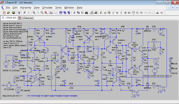
The result is as expected, it does not differ very much from the one obtained with the Middlebrook voltage probe.
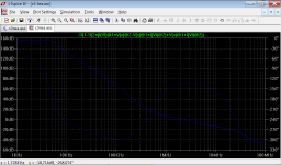
If one deletes the E block E2 from the circuit, the result looks as follows.
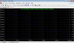
Two explanations come into my mind:
1. Is this some kind of rounding error in the calculations?
2. Does it show a feed-forward path through the feedback networks? The gain of the circuit is huge, and the impedance ratios of feedback pathes and upper limit of output impedance are only in the order of 60 dB (if not less). Maybe, it is even a path between the different feedback branches.
So, I will follow these two lines. Independently of the result, I'm already grateful to David that you urged me to improve the measurement techniques.
Did anybody else already see such an effect?
Kind regards,
Matthias
PS. How does one include such a nice self-magnifying figure?
Following David's advice, I have started to use the probe by Tian et al.
I will discuss the issues raised (e.g. probing at bases of Q7 and Q13) later, from a first look there are no effects that cannot be fine-tuned in a next circuit version.
The real surprise comes from another side: when probing the total loop gain around the output stage (last of the plots in post #45), I cannot exclude that there is a feed-forward path through the feedback networks. This is seen as follows.
In the next image, the schematic with Tian probe around the output stage is shown, together with an E block (voltage-controlled voltage source) that restricts signals to flow from circuit output backward to the feedback network.

The result is as expected, it does not differ very much from the one obtained with the Middlebrook voltage probe.

If one deletes the E block E2 from the circuit, the result looks as follows.

Two explanations come into my mind:
1. Is this some kind of rounding error in the calculations?
2. Does it show a feed-forward path through the feedback networks? The gain of the circuit is huge, and the impedance ratios of feedback pathes and upper limit of output impedance are only in the order of 60 dB (if not less). Maybe, it is even a path between the different feedback branches.
So, I will follow these two lines. Independently of the result, I'm already grateful to David that you urged me to improve the measurement techniques.
Did anybody else already see such an effect?
Kind regards,
Matthias
PS. How does one include such a nice self-magnifying figure?
Hi Matthias,
What happens if you change from TMC to TPC (network R6, C1, C8). Is there a path through C1 and R6? Also Wondering whether a Tian probe in line with R6 could tell us anything useful?
What worries me about TMC are the extra loops it creates when compared to TPC. There is more chance of creating strange anomalies...
Paul
The real surprise comes from another side:
...
Two explanations come into my mind:
1. ...error in the calculations?
Round-off error looks very unlikely as an explantion
As I said earlier, at first I believed the surprise results were a quirk of LTspice and did not take them seriously.
Then I realized that usually it looked "funny" because I did not understand the circuit correctly.
So now I assume the LTSpice is correct unless I see proof otherwise.
In that case a result may be unexpected because
1. You have plotted the expected variable but it's value is not expected.
2. The plot is not the variable you expected. Then the issue is whether the result has some physical relevance.
This is why I recommend the Tian technique. There is clear physical relevance for a Return Ratio directly at the transistor.
The RR/Loop Gain in some arbitrary path is often of dubious usefulness.
2. Does it show a feed-forward path... Maybe, it is even a path between the different feedback branches.
Probably. Bode (as usual) was aware of this effect and discusses it.
He points out essentially the same as your comment, that when there is a lot of gain between sections then even usually trivial feed-forward paths can become important.
4 section architectures have extra connections to worry about and so are more prone to this complication, hence my reluctance to use them for audio.
IC people do use them, but only when they are forced to by low power rails.
PS. How does one include...
Use the "postcard" icon to insert the picture rather than "paper-clip" icon to add it as an attachment.
Best wishes
David
Last edited:
... from TMC to TPC (network R6, C1, C8).
Excellent question for an experiment.
I suspect the effect is not due to the prevention of forward transmission around the OPS by the V source, but rather it's zero impedance.
Note that there is a positive feedback path via C8 R6 C7 C9 back to Q7.
Would it not short this transmission path?
What worries me about TMC are the extra loops it creates when compared to TPC....
Especially when combined with 4 sections
As I wrote, I don't care about the extra transistors but I worry about unforeseen interactions.
On the positive side, if we can analyse "4 section with TPC nested within TMC" then conventional amps will be easy.
Best wishes
David
Hi Paul and David,
thank you for the thoughts and proposals. I will try out things, but need to slow down a bit.
There is only one test I want to report on: in the circuit from post #73, I have included a resistor between output of the isolating E block E2 and node y. Thus, feed-forward via the output stage still is blocked, but interaction between the three feedback branches is possible.
Even with a value of 0.1 Ohm, which is a rather low estimate of the (open-loop) OPS output impedance, the behaviour with gain peak above 10 kHz shows up. So, very probably, there is an interaction between the three feedback branches.
That's interesting. I thought that a chair on three legs does stand stable.
Kind regards,
Matthias
There is only one test I want to report on: in the circuit from post #73, I have included a resistor between output of the isolating E block E2 and node y. Thus, feed-forward via the output stage still is blocked, but interaction between the three feedback branches is possible.
Even with a value of 0.1 Ohm, which is a rather low estimate of the (open-loop) OPS output impedance, the behaviour with gain peak above 10 kHz ...
So if I understand you then that supports exactly what I wrote?
You can also move the one-way buffer into the various loops.
... that a chair on three legs does stand stable.
Not a very helpful equivalence I think
Three way connections complicate the feedback, usually for the worse (feedforward and potential RHP zeroes)
Best wishes
David
Yes. But I will do that first with a conceptual version of the circuit (E and G elements). The peak reminds me somehow to the one in a "classical" topology with TPC; have to admit that I never really understood it.So if I understand you then that supports exactly what I wrote?
You can also move the one-way buffer into the various loops.
Matthias
Medium-power amplifier
Based on the design from post #45, I have tried to make some improvements. My goal is to build such a medium-power amp as next "real" project after the wired, but still nicely playing low-power amp from post #1. It would operate from +/- 25V rails with total quiescent current of around 100mA and hopefully produce 25W of clean power into 4R.
The output stage and "VAS" follow the common text book configuration, but no doubling of power transistors or triple driver configuration is used. The unity loop gain frequency (ULGF) seen in total by the output stage is around 2MHz. Simulation results in safely less than 1ppm distortion from 0 to 25W into 4R at 20kHz, measured up to 100kHz. At not much lighter loads, distortion is dominated by the input and intermediate stages.
Figure 'schematic.png' shows the overall circuit. I have reworked the intermediate stage with the three transistors Q1, Q9 and Q8 together with current source Q10/Q11. So it was possible to add an additional feedback path via R53 and C21 that produces 20dB more negative feedback at 50kHz. It is probably difficult to call this still a nested Miller compensation loop. Besides a name, closing a further loop only one -- common base operated -- transistor next to the VAS input is quite nice ;-).
The PSRR is not yet optimal at lower frequencies. Therefore, I will probably add some "active filtering" for the VAS and small signal stage supply voltages.
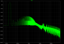
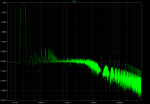
For 25W and 0.25W into 4R, figures 'thd20-10V.png' and 'thd20-1V.png' show the output spectra.
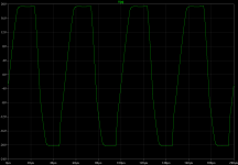
Clipping (24V) in figure clipping.png seems acceptable. The circuit contains elements to avoid destructive overload of small signal stages; this also improves clipping. Given the high-order feedback applied, the relatively smooth clipping behaviour nevertheless is surprising.
Perhaps, it will be possible to turn the whole circuit silently on and off by simultaniously enabling or disabling the two current sources around Q5 (input stage) and Q15 (VAS). This would also be valuable for a protection circuit.
I'm quite content that all transistors either enjoy good emitter degeneration or a local linearizing loop, e.g. the loop with Q1 and Q9 and of course the VAS loop. Furthermore good stability margins are achieved, e.g. around 20dB gain margin with "smooth curves" in all loops. This was possible without small capacitors e.g. parallel to R13 (global NFB), or R21 (next-inner loop), or R5 (driving from intermediate stage into summing point of subsequent feedback loop). The trick is the small inductivity L2 in the feedback loop at the output of the intermediate stage. It "shifts some stability margin" from a place with enough reserve to the front stages.
Tian et.al. probes for the bases of all small signal stages (Q8: emitter) and around the output stage look nice. This also holds for the inner loop with Q1 and Q9 as well as the VAS loop with Q13 and Q14 (with rest of circuit being in in normal aperation). On interest, I can show that in another post.
Currently, I'm playing with a cascoded JFET input stage. Since the amp shall be connected directly to a 10k volume pot, changing source impedance is an issue. First experiments suggest that the high capacities of the 2SK389 pose a problem. On the other hand, LS844 seems to be well suited, since the circuit does not need high transconductance in the input stage. Achieving the low BJT stage distortion with 20V rail voltage at 1V signal swing appearently is not that easy.
An always open topic is of course the output stage. I do not want to use more "heavy hardware" and would like to stay with 2MHz ULGF and 0.22R emitter resistors for good thermal stability. Is there still something to be improved, apart from the Vbe multiplier?
VAS current seems to be low at 5mA, but an increase does not really bring a benefit.
Until now, I have not found better drivers than BD139/140. They are linear, fast, and the SOA region is large enough.
ULGF in the TMC loop via R6 is 600kHz, as in the other loops. Maybe, one can increase this frequency, since stability margins are excellent and can be further improved by a small R+C parallel to R6. But this of course would also raise the total ULGF seen be the output transistors.
Matze
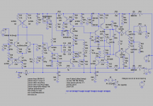
(Perhaps these attachments do not work as intended. I'm sorry; haven't been here for quite some time.)
Based on the design from post #45, I have tried to make some improvements. My goal is to build such a medium-power amp as next "real" project after the wired, but still nicely playing low-power amp from post #1. It would operate from +/- 25V rails with total quiescent current of around 100mA and hopefully produce 25W of clean power into 4R.
The output stage and "VAS" follow the common text book configuration, but no doubling of power transistors or triple driver configuration is used. The unity loop gain frequency (ULGF) seen in total by the output stage is around 2MHz. Simulation results in safely less than 1ppm distortion from 0 to 25W into 4R at 20kHz, measured up to 100kHz. At not much lighter loads, distortion is dominated by the input and intermediate stages.
Figure 'schematic.png' shows the overall circuit. I have reworked the intermediate stage with the three transistors Q1, Q9 and Q8 together with current source Q10/Q11. So it was possible to add an additional feedback path via R53 and C21 that produces 20dB more negative feedback at 50kHz. It is probably difficult to call this still a nested Miller compensation loop. Besides a name, closing a further loop only one -- common base operated -- transistor next to the VAS input is quite nice ;-).
The PSRR is not yet optimal at lower frequencies. Therefore, I will probably add some "active filtering" for the VAS and small signal stage supply voltages.
For 25W and 0.25W into 4R, figures 'thd20-10V.png' and 'thd20-1V.png' show the output spectra.
Clipping (24V) in figure clipping.png seems acceptable. The circuit contains elements to avoid destructive overload of small signal stages; this also improves clipping. Given the high-order feedback applied, the relatively smooth clipping behaviour nevertheless is surprising.
Perhaps, it will be possible to turn the whole circuit silently on and off by simultaniously enabling or disabling the two current sources around Q5 (input stage) and Q15 (VAS). This would also be valuable for a protection circuit.
I'm quite content that all transistors either enjoy good emitter degeneration or a local linearizing loop, e.g. the loop with Q1 and Q9 and of course the VAS loop. Furthermore good stability margins are achieved, e.g. around 20dB gain margin with "smooth curves" in all loops. This was possible without small capacitors e.g. parallel to R13 (global NFB), or R21 (next-inner loop), or R5 (driving from intermediate stage into summing point of subsequent feedback loop). The trick is the small inductivity L2 in the feedback loop at the output of the intermediate stage. It "shifts some stability margin" from a place with enough reserve to the front stages.
Tian et.al. probes for the bases of all small signal stages (Q8: emitter) and around the output stage look nice. This also holds for the inner loop with Q1 and Q9 as well as the VAS loop with Q13 and Q14 (with rest of circuit being in in normal aperation). On interest, I can show that in another post.
Currently, I'm playing with a cascoded JFET input stage. Since the amp shall be connected directly to a 10k volume pot, changing source impedance is an issue. First experiments suggest that the high capacities of the 2SK389 pose a problem. On the other hand, LS844 seems to be well suited, since the circuit does not need high transconductance in the input stage. Achieving the low BJT stage distortion with 20V rail voltage at 1V signal swing appearently is not that easy.
An always open topic is of course the output stage. I do not want to use more "heavy hardware" and would like to stay with 2MHz ULGF and 0.22R emitter resistors for good thermal stability. Is there still something to be improved, apart from the Vbe multiplier?
VAS current seems to be low at 5mA, but an increase does not really bring a benefit.
Until now, I have not found better drivers than BD139/140. They are linear, fast, and the SOA region is large enough.
ULGF in the TMC loop via R6 is 600kHz, as in the other loops. Maybe, one can increase this frequency, since stability margins are excellent and can be further improved by a small R+C parallel to R6. But this of course would also raise the total ULGF seen be the output transistors.
Matze


(Perhaps these attachments do not work as intended. I'm sorry; haven't been here for quite some time.)
- Status
- This old topic is closed. If you want to reopen this topic, contact a moderator using the "Report Post" button.
- Home
- Amplifiers
- Solid State
- Amplifier with nested Miller compensation