I saw this a couple of days ago and started to draw it up. Another entertaining design Elvee. When I looked again mickeymoose had offered to lay out a board.
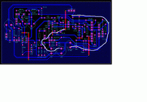
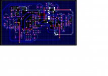
Here's my stab at it, I've used a 4-way header for the connections to the heatsinked components. As per my usual practise I've filled the unused areas with groundplane, but with a generous clearance, to make for easy assembly if etching at home, but also to save on etchant. All tracks are 50 thou. The board is no particular size (4.45*2.6 in), just the size it came out, I could probably tweak it down a bit smaller, but why? There's a bit more clearance at the edges than is absolutely necessary.

I went with the packages my schematic tool had built in. The board is obviously single-sided, with half-a-dozen wire links. I've used capacitor pakckages that will accommodate 2 different sizes in the non-electrolytics, the electrolytics are all radial packages which should be big enough, but again I'd be re-checking this when I had the components in hand if I was doing the build myself.

Some component designations are changed from the original, and of course some errors may have crept in in transcription.
I won't be building one myself in the immediate future so if anybody does want to work from this layout you better scrutinize the board pretty closely for anything you object to and get back to me for modifications.
Graphicode's free GC-Prevue should pretty much swallow (import) the whole .zip file, it'll balk at a couple of places, the drill file, just keep going yes, OK.
View attachment circlophone - CADCAM.ZIP
w
Here's my stab at it, I've used a 4-way header for the connections to the heatsinked components. As per my usual practise I've filled the unused areas with groundplane, but with a generous clearance, to make for easy assembly if etching at home, but also to save on etchant. All tracks are 50 thou. The board is no particular size (4.45*2.6 in), just the size it came out, I could probably tweak it down a bit smaller, but why? There's a bit more clearance at the edges than is absolutely necessary.
I went with the packages my schematic tool had built in. The board is obviously single-sided, with half-a-dozen wire links. I've used capacitor pakckages that will accommodate 2 different sizes in the non-electrolytics, the electrolytics are all radial packages which should be big enough, but again I'd be re-checking this when I had the components in hand if I was doing the build myself.
Some component designations are changed from the original, and of course some errors may have crept in in transcription.
I won't be building one myself in the immediate future so if anybody does want to work from this layout you better scrutinize the board pretty closely for anything you object to and get back to me for modifications.
Graphicode's free GC-Prevue should pretty much swallow (import) the whole .zip file, it'll balk at a couple of places, the drill file, just keep going yes, OK.
View attachment circlophone - CADCAM.ZIP
w
Thanks for your work, Wakibaki, ")
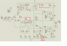
I have spotted one or two small errors in the schematic, see below.
About the layout, I'm a bit unhappy with the daisy-chaining of the power tracks towards the decoupling capacitors.
It would be better to place C8 near D8, R12, J3-1 and C10 near D9, R24, R13, J3-3, and start from there to distribute the supplies to the low-power circuits.
I have highlighted in white the tracks in question.
Apart from that, everything looks OK.
Attachments
Sorry about the double post, I inadvertently reloaded the page.
Revised circuit:

Positive power distribution:

Negative power distribution:

Gerber:
View attachment circlophone_fix_1 - CADCAM.ZIP
w
Revised circuit:
Positive power distribution:
Negative power distribution:
Gerber:
View attachment circlophone_fix_1 - CADCAM.ZIP
w
Found some definite errors, missing links on the dual pin 1's of the dual size cap packages.

View attachment circlophone_fix_2 - CADCAM.ZIP
w
View attachment circlophone_fix_2 - CADCAM.ZIP
w
I see a possible improvement, if you don't mind:
The area enclosed by Q12, Q13, R21 and D9 makes me a bit nervous.
This can be avoided by placing R21 differently:
Edit:
I have just seen that Q10 & Q11 have their emitter and collector swapped.
The area enclosed by Q12, Q13, R21 and D9 makes me a bit nervous.
This can be avoided by placing R21 differently:
Edit:
I have just seen that Q10 & Q11 have their emitter and collector swapped.
Attachments
Last edited:
Thanks!Congratulations.
Yeah, they are a bit on the slow side, but the SOAR is phenomenal.2N6259 very nice
these are some of the most robust transistors EVER made from GE/RCA. probably similar Ft's to the original 2N3055 but 4X the die size.
I have made some tests to evaluate the actual necessity of an inductive Zobel.
I have tried increasing values of capacitance starting with 47nF, 100nF, ... up to 2.2µF, directly connected to the output through 25cm leads (10in).
Pure capacitance, no parallel or series damping resistor, test signal a 10KHz triangle of maximum amplitude.
There were no signs of instability, distortion, or anything else.
In conclusion, I think that such a network is not needed in 99.9% of the cases.
Exceptions might be a combination of very exotic speaker cables and exotic loudspeakers, not the kind of target for this simple amplifier.
I really intend to build this thing. I have been getting into designing PCB layouts lately, and I feel I am getting good at it. I gave it a go designing one for this, but gave up about 75% of the way through. Not at that point of learning just yet. I have been doing small preamps, opamp circuits, power supplies and the like. So, If a good final pcb is created, I will test it after a few people (Elvee) eye it up and give it a (preliminary) OK.
I have one important question, though. Elvee, what are good through hole substitutes for the SMD diodes? I can purchase the smd parts and use them just fine, but it seems that the PCB being made here (the only one so far) is going to use through-hole parts.
I still have to do an inventory of transistors to see what I've got, but I'm sure I've got the parts I need besides those few diodes. I am comfortable if needed to use the faster devices for the OP transistors and tweak it for stability... another opportunity to learn.
The diodes are not at all critical. Let us leave aside the 1N4148, I don't think this could cause problems.I have one important question, though. Elvee, what are good through hole substitutes for the SMD diodes? I can purchase the smd parts and use them just fine, but it seems that the PCB being made here (the only one so far) is going to use through-hole parts.
There is one small signal schottky, the BAT54. In fact, I should have specified a BAT81 or BAT85, as it is a TH design.
It is absolutely non-critical, and any 30V - 200mA schottky will do.
There also is a 1N5xxx suitable, but at the moment, I don't remember the type number.
If you don't have a schottky available, you could even use a 1N4148.
The larger schottky's can be almost anything, BYS45, 1N5820, ... with Imax>=3A.
You could even use a fast silicon diode, BYV31 or similar: it would only affect the swing (energetic efficiency)
I still have to do an inventory of transistors to see what I've got, but I'm sure I've got the parts I need besides those few diodes. I am comfortable if needed to use the faster devices for the OP transistors and tweak it for stability... another opportunity to learn.
The transistors are not critical either: they just need to have sufficient ratings for the job.
And if you confine yourself to calm, placid transistors like the 2N3055, you will not encounter any problem.
And when you're confident enough, you can begin to tweak and use faster devices.
Basically, this amplifier is designed to be tolerant and undemanding regarding the components.
There are one or two things to care about though, f.e. the collector capacitance of Q5 and Q6: if you use high capacitance devices (>20pF), you will most likely ruin the performance.
I'll try to come up with a formal builder's guide, to make those (few) things clear.


View attachment circlophone_fix_3 - CADCAM.ZIP
w
If you see anything else don't hesitate to point it out.
View attachment 225174
View attachment 225180
View attachment 225181
w
If you see anything else don't hesitate to point it out.
Thank you for that. I have created pdfs from the files for my own use if anybody wants me to post them. One pdf of the board with bottom, drill, and top silk screen layers. One pdf of the bottom and drill layers in black and white. Both 1:1 scale. I just realized I didn't include the top layer with the jumper wires.
The Circlophone© builder's notes
Here is a compendium of useful information for would-be builders
- Input:
The input resistance is approximately 10K.
But, the source impedance must be kept well below that value.
This is because the tail current of the input pair is dynamically modulated by the bias servo, and any imbalance in the input impedances will generate a parasitic voltage due to the bias currents of the input transistors.
This will cause a "leak" of the common mode signal into the "noble" differential path, and will increase the distortion.
For this reason, source impedances much greater than 1K should be avoided.
In practice, this means that if a volume pot is placed directly in front of the amplifier, its value should be 4.7K or less.
If the input is fed from a preamplifier, the impedance will normally be in the hundreds of ohms, which is optimal.
Q3 and Q4 can be any small signal PNP with a Vceo>Vs, BC556 or 557 f.e.
For the above-mentionned reasons, a high Hfe type is preferable, as it will minimize the effects of the bias current (suffix "C" for BCxxx).
Q1 is identical.
C6/R23 are the main compensation components of the amplifier. On some versions I have used 22 ohm for R23, on other 33 ohm, and in the end I settled for 27 ohm, as I was not sure what the best value was. Anyway it is not critical, and either value will work.
1.5nF seems to be the optimum for C6.
- Phase splitter:
Q5 and Q6 must be rated at 2Vs, and their average dissipation is 13mA*Vs.
TO5 or TO39 types are ideally suited, as their free air dissipation is generally 800mW, which is sufficient for 50V supplies. Suitable examples are 2N3019, 2N3053, 2N1893 and 2N2219 (for low voltages).
It is important to use relatively low capacitance types (Ccb<15pF).
The zeners equalize the dissipation between the two transistors, they should total approximately Vs.
For Q13 a Vceo>2Vs is required.
- Drivers:
Medium power transistors similar to the BD140 are perfect for Q9 and Q11. A Vceo>2Vs is required, and depending upon the power of the amplifier, they could dissipate up to 5W.
- Output:
For powers up to 50W, 2N3055 are perfect. Vceo has to be greater than 2Vs, and they need adequate cooling. The SOAR must also be sufficient.
With such slow devices, C11 is optional and C12 can safely be reduced to 180pF.
These capacitors ensure local stability, but at the expense of the global loop's margins.
This means that being too heavy-handed is counter-productive, and excessive values will degrade the transient response.
With faster devices (Ft>4Mhz), C11 becomes mandatory, and C12 needs to be increased, up to 820pF.
The values of the capacitive Zobel look like a misprint, but they aren't: the output topology is unconventional, and these values give the best results. On some prototypes, I have also used 4.7 ohm for R25.
- General:
Other transistors need no special mention, and the role of the power schottky's is simply to limit the power wasted, they have no active role.
The power supply voltage can range from less than 15V to more than 50V, provided suitable devices are used.
Only the zeners need to be adapted, and also R21, to keep the current within the 1mA to 2mA limits.
All resistors are 0.25W, and no selection, matching or thermal tracking between any components is required to obtain the advertised performances.
As with any amplifier, good layout practices are recommended, particularly for the ground and output nodes.
Last edited:
Here is a compendium of useful information for would-be builders
- Input:
The input resistance is approximately 10K.
But, the source impedance must be kept well below that value.
This is because the tail current of the input pair is dynamically modulated by the bias servo, and any imbalance in the input impedances will generate a parasitic voltage due to the bias currents of the input transistors.
This will cause a "leak" of the common mode signal into the "noble" differential path, and will increase the distortion.
For this reason, source impedances much greater than 1K should be avoided.
In practice, this means that if a volume pot is placed directly in front of the amplifier, its value should be 4.7K or less.
If the input is fed from a preamplifier, the impedance will normally be in the hundreds of ohms, which is optimal.
Q3 and Q4 can be any small signal PNP with a Vceo>Vs, BC556 or 557 f.e.
For the above-mentionned reasons, a high Hfe type is preferable, as it will minimize the effects of the bias current (suffix "C" for BCxxx).
Q1 is identical.
C6/R23 are the main compensation components of the amplifier. On some versions I have used 22 ohm for R23, on other 33 ohm, and in the end I settled for 27 ohm, as I was not sure what the best value was. Anyway it is not critical, and either value will work.
1.5nF seems to be the optimum for C6.
- Phase splitter:
Q5 and Q6 must be rated at 2Vs, and their average dissipation is 13mA*Vs.
TO5 or TO39 types are ideally suited, as their free air dissipation is generally 800mW, which is sufficient for 50V supplies. Suitable examples are 2N3019, 2N3053, 2N1893 and 2N2219 (for low voltages).
It is important to use relatively low capacitance types (Ccb<15pF).
The zeners equalize the dissipation between the two transistors, they should total approximately Vs.
For Q13 a Vceo>2Vs is required.
- Drivers:
Medium power transistors similar to the BD140 are perfect for Q9 and Q11. A Vceo>2Vs is required, and depending upon the power of the amplifier, they could dissipate up to 5W.
- Output:
For powers up to 50W, 2N3055 are perfect. Vceo has to be greater than 2Vs, and they need adequate cooling. The SOAR must also be sufficient.
With such slow devices, C11 is optional and C12 can safely be reduced to 180pF.
These capacitors ensure local stability, but at the expense of the global loop's margins.
This means that being too heavy-handed is counter-productive, and excessive values will degrade the transient response.
With faster devices (Ft>4Mhz), C11 becomes mandatory, and C12 needs to be increased, up to 820pF.
The values of the capacitive Zobel look like a misprint, but they aren't: the output topology is unconventional, and these values give the best results. On some prototypes, I have also used 4.7 ohm for R25.
- General:
Other transistors need no special mention, and the role of the power schottky's is simply to limit the power wasted, they have no active role.
The power supply voltage can range from less than 15V to more than 50V, provided suitable devices are used.
Only the zeners need to be adapted, and also R21, to keep the current within the 1mA to 2mA limits.
All resistors are 0.25W, and no selection, matching or thermal tracking between any components is required to obtain the advertised performances.
As with any amplifier, good layout practices are recommended, particularly for the ground and output nodes.
Great! I just found a whole bunch of MJ802's. They are even a bit (2MHZ) slower than the 3055's, but more robust.
odysseybmx414, kindly post the pdf of the board...thanks
Elvee, is the schematics of this clever amp can be adopted to Nch Vfets output? I ask since I have bunch of those 2sk's. i want to try building this BJT version and Vfet if possible...thanks
Here ya go:
http://dl.dropbox.com/u/5430178/circlophone/circlophone_fix_3 - Bottom Black_With Drill.pdf
http://dl.dropbox.com/u/5430178/cir...ix_3 - Bottom Copper_Drill_Top Silkscreen.pdf
Keep in mind I forgot the layer with the jumper wires. But you can look at wakabaki's posted thumbnail for those.
EDIT: Temporarily ignore those. I just noticed what I think is a big error.
Wakabaki, your thumbnail shows several traces that are not seperated at all from the groundplane that surrous them. In the gerber files, they do not show up at all. Am I missing something?
Last edited:
There is no reason why it couldn't: to show the flexibility of the concept, I had given an example based on N-darlingtons here:odysseybmx414, kindly post the pdf of the board...thanks
Elvee, is the schematics of this clever amp can be adopted to Nch Vfets output? I ask since I have bunch of those 2sk's. i want to try building this BJT version and Vfet if possible...thanks
http://www.diyaudio.com/forums/solid-state/189599-my-little-cheap-circlophone-2.html#post2585337
Going from N-darlington to N-MOS is a very small step, it just involves adapting the 120ohm B-E resistors to a value compatible with the G-S threshold voltage of the MOS you use.
Very minor indeed.
A drawback of this straight modification is that the output swing would be amputated of ~Vth at high current on the positive side, something like 4V.
Note that the only types of amplifiers that were actually built are based exclusively on bipolars, PNP drivers and NPN output, the rest is only simulation.
Avoiding the asymmetrical swing could be achieved by combining the topologies of the Circlophone and the CircloMOS, but it would be somewhat more complex than merely adapting a resistor value.
I think you are talking about the ground tracks connected to the ground plane by thermal reliefs.Wakabaki, your thumbnail shows several traces that are not seperated at all from the groundplane that surrous them. In the gerber files, they do not show up at all. Am I missing something?
- Home
- Amplifiers
- Solid State
- ♫♪ My little cheap Circlophone© ♫♪