Since inverting-mode circuits seem to be gaining in popularity recently, I decided to post a circuit which is fairly simple and may be interesting for someone. The idea itself is old, but I don't see many circuits utilizing this method today.
The core idea is to use the gates/bases of JFET/BJTs for the signal inputs (per normal practice), but route the NFB loops through the sources/emitters of the same devices. If nothing else, this should allow one to utilize various inverting feedback configurations without having to rely on high-impedance series-input resistors for fear of loading down the source component excessively.
Obviously, this theme can be combined with many other ideas - complementary input stages, cascoding, active loading, folded cascode or current-mirror second stage, higher rail voltages, multiple output devices, etc.
No oddball devices have been used, and resistive loading has been used throughout, so it should be fairly easy to make. I settled on Toshiba for all of the semiconductor devices, and there are only 4 types of active devices used. Note I haven't built this yet, but I think that the values should be reasonably close to functional. But please be prepared to do at least _some_ tuning/troubleshooting/tweaking.
Apologies in advance for any errors.
regards, jonathan carr
Attachments
I have put this interesting JFET-MOS-BTL-amplifier Circuit in my FTP-server.jcarr said:Since inverting-mode circuits seem to be gaining in popularity recently, I decided to post a circuit which is fairly simple and may be interesting for someone. The idea itself is old, but I don't see many circuits utilizing this method today.
The core idea is to use the gates/bases of JFET/BJTs for the signal inputs (per normal practice), but route the NFB loops through the sources/emitters of the same devices. If nothing else, this should allow one to utilize various inverting feedback configurations without having to rely on high-impedance series-input resistors for fear of loading down the source component excessively.
Obviously, this theme can be combined with many other ideas - complementary input stages, cascoding, active loading, folded cascode or current-mirror second stage, higher rail voltages, multiple output devices, etc.
-----------------------
regards, jonathan carr
Filename: jcarr_BTL_FET-AMP_v1.gif
It is in size to fit a 1024x768 screen.
I call it v1 - version 1.
Also have put - jcarr and his website URL - as added text into the image.
-----------------------------------------------
Thanks Jonathan!
on behalf of us all.
")
/halo - and the rest of the pack will come after you, if the amp doesn't work

Halojoy:
>and the rest of the pack will come after you, if the amp doesn't work<
You are an excellent designer, my friend. Already you have deduced the reason why I set the voltage rails at +/-15V.
If you want to be careful, +/-12V could be an even better starting point... ROTFLOL!
jonathan carr
>and the rest of the pack will come after you, if the amp doesn't work<
You are an excellent designer, my friend. Already you have deduced the reason why I set the voltage rails at +/-15V.
If you want to be careful, +/-12V could be an even better starting point... ROTFLOL!
jonathan carr
An exciting moment lies ahead
When the first one to test this amp in real life
posts his results and findings.
I guess it will be one of them pass-boys.
They are the ones having piles and piles of MOSFETs & JFETs
along most walls in their livingspace.
And their bathtub is filled with 100.000uF Electrolytes - big as BEER-CANS.
Their kitchen drawers and wardrobes are full with
Toroid transformers, so BIG & HEAVY
that it takes 2 fullgrown men, to move them some inches at the time.
They will probably be in touch here in a couple of days.
/halo - thinks them pass-boys are some special kind of species
A very exciting moment lies ahead of us:jcarr said:Halojoy:
>and the rest of the pack will come after you, if the amp doesn't work<
You are an excellent designer, my friend. Already you have deduced the reason why I set the voltage rails at +/-15V.
If you want to be careful, +/-12V could be an even better starting point... ROTFLOL!
jonathan carr
When the first one to test this amp in real life
posts his results and findings.
I guess it will be one of them pass-boys.
They are the ones having piles and piles of MOSFETs & JFETs
along most walls in their livingspace.
And their bathtub is filled with 100.000uF Electrolytes - big as BEER-CANS.
Their kitchen drawers and wardrobes are full with
Toroid transformers, so BIG & HEAVY
that it takes 2 fullgrown men, to move them some inches at the time.
They will probably be in touch here in a couple of days.
/halo - thinks them pass-boys are
some special kind of species jcarr Special amp
Here is Jonathan's interesting Amplifier!
Balanced 2SK389 JFET in - Bridged MOSFET out !!!!!!!!!
- What more do we need?
Help Jonathan to modify and test it. Might be a real Classic Amp in time.
larger image in the zip above
or at my collection below
/halo
Here is Jonathan's interesting Amplifier!
Balanced 2SK389 JFET in - Bridged MOSFET out !!!!!!!!! - What more do we need?
Help Jonathan to modify and test it. Might be a real Classic Amp in time. larger image in the zip above
or at my collection below
/halo
Attachments
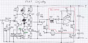
For the audio archaeologists, I found a somewhat peculiar
variation on this method when reverse engineering a friends
old preamplifier a while ago. Instead of feeding the signal back
directly into the source circuit, there is a BJT in series with the
source, and the feedback drives this BJT. Maybe there is some
good idea behind this, but it seems to me that this is likely to
introduce unnecessary non-linearities.
The design from the early or mid 80s and Sentec are not
even in the audio business anymore, so I guess I won't do
any harm to post my schematic of it. Note that I have broken
the feedback path in the drawing, and marked it with "a".
Attachments
Thanks Christer
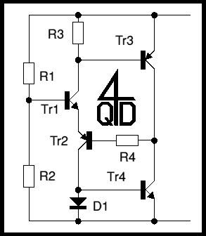
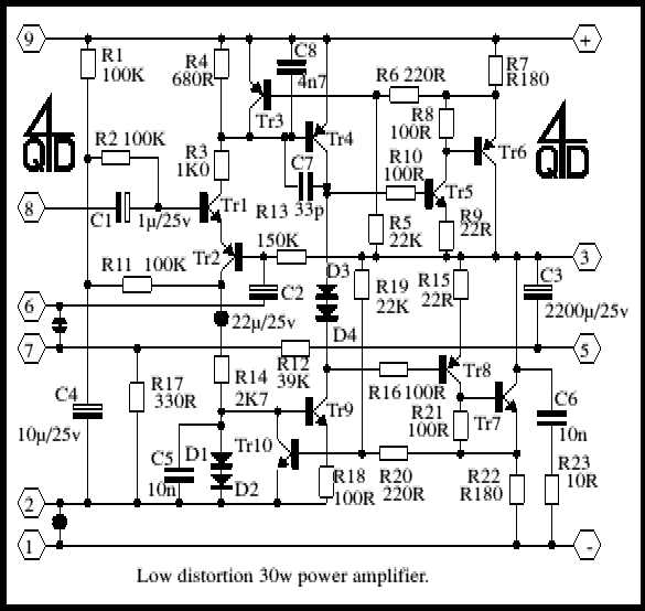
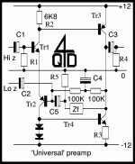
The same you can find as a general design-idea at 4QDTEC.
In fact the name 4QD refers to this basic configuration of amplifier.
4 transistors(Q) design.
--------------------------------------------------------------
The basic circuit princip, opamp, is found on this page:
http://www.4qdtec.com/opamp.html
Here in a preamp version:
http://www.4qdtec.com/preamp.html
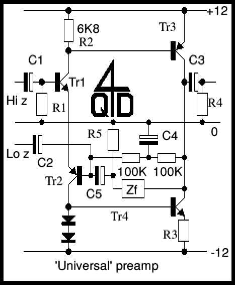
Same cofiguration used in a Low Distortion 30Watt PowerAmp:
http://www.4qdtec.com/pwramp.html
/halo your living amplifier librarian
Thanks Christer!Christer said:For the audio archaeologists, I found a somewhat peculiar
variation on this method when reverse engineering a friends
old preamplifier a while ago. Instead of feeding the signal back
directly into the source circuit, there is a BJT in series with the
source, and the feedback drives this BJT. Maybe there is some
good idea behind this, but it seems to me that this is likely to
introduce unnecessary non-linearities.
The same you can find as a general design-idea at 4QDTEC.
In fact the name 4QD refers to this basic configuration of amplifier.
4 transistors(Q) design.
--------------------------------------------------------------
The basic circuit princip, opamp, is found on this page:
http://www.4qdtec.com/opamp.html
Here in a preamp version:
http://www.4qdtec.com/preamp.html
Same cofiguration used in a Low Distortion 30Watt PowerAmp:
http://www.4qdtec.com/pwramp.html
/halo
your living amplifier librarianThanks Halo, I did not know about that site. Interestingly,
the site owner says about this design that "It is a circuit which
is original to me and I have never seen its like used elsewhere!"
It is not clear, however, if he "invented" it himself, or got it from
somewhere, this somwhere being the only place he has seen
it. Unless he invented it 20 years ago, it obviously was around
before, though.
He also makes an interesting remark that the input NPN and
PNP transistors actually form a LTP (diff. pair). Well, that seems
reasonable. It should be noted, however, that the Sentec
design I posted differs by using a JFET/BJT combination. It
pretty much boils down to the same principle, but it seems it
would have made more sense to use two JFETS then, or two
BJTs. I am sure there was some clever intention with this, though.
I actually remember visiting Sentec, together with another friend,
when this amps was new and we discussed it with them. Of
course, we did not know the topology of the amp then, but
I remember the guy we talked to giving a good impression.
They seemed to take a lot of care in selecting components
for instance. I even think he said something about inventing
some new electronics theory, which could have been related
to this input design, perhaps. Anyway, they seemed very proud
of the input stage at the time.
There are both possible advantages and disadvantages with this configuration of feedback.Christer said:Thanks Halo
It should be noted, however, that the Sentec
design I posted differs by using a JFET/BJT combination. It
pretty much boils down to the same principle, but it seems it
would have made more sense to use two JFETS then, or two
BJTs. I am sure there was some clever intention with this, though.
The great poopularity of the longtailed pair is much due to the low offset.
This avoids the use of either input or output capacitor. Or avoids both of them.
It is also great for the input bias resistor, only to be connected to ground, common, in a dual supply circuit. (gives Power Supply Rejection without filters).
The idea of using one JFET and one BJT is to me obvious.
I have had the same idea myself, when I first visited
4QD-site some years ago.
If you select a current where g-s voltage is equal negative
as the bjt is positive (0.7 volt)
you cancel the DC-offset between input and output.
This means you can have the amplifier DC in DC out,
and only use one input resistor to common.
This is the hard part:
Of course you will have to find both a JFET and BJT smallsignal transistor, that work well
at that same current, with the same amount of opposite voltage drop.
jfet n + bipolar p
OR
jfet p + bipolar n
Jfet have negative Vgs
Bipolar have positive Vbe
/halo
Halo,
I don't quite see the advantage. It would be much easier to
match a complementary pair of BJTs or a complementary pair
of JFETS. The Vgs of a JFET at the operating point is usually
higher than the Vbe of a BJT. I never had a chance
to do any measurements on the amp, and I haven't tried to
calculate anything on it or simulate it, but my guess is that
the feedback signal would normally have a negative
DC offset in order to match up the Vgs of the JFET. It seems
to me that using a pair of devices with different characteristics
as a pair will introduce unnecessary non-linearities. Well, what
do I know. Maybe some of the gurus can figure out why they
did it this way.
advantages
Christer
I guess your judgement of this technique is the correct one.
If this was, from the HiFi quality aspect, a better way,
we would see lot of this in good amplifiers.
The advantage is probably more on the practical level.
And it saves some components.
At least in 4QD basic circuit, you do not need any separate constant current source. Saves some transistor and resistors.
But adds some capacitors and 1.2 volt DC-offset.
/halo
Attachments
Still, there must be some reason why Sentec did what they did.
I don't believe they did it to save the cost of a transistor. These
were not cheap amplifiers, although not extreme in any way.
Furthermore, the predecessor from the late 70s did use
mirror-image symmetrical diff pairs with current sources and
current mirrors, if I remember correctly, so they had experience
with the "traditional" approach before.
This is beginning to look as if we are threadjacking, although it
is related to Jonathans original circuit, which is why I posted it.
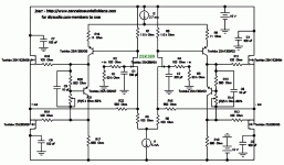
Better we get on track with the Original Subject:jcarr said:The core idea is to use the gates/bases of JFET/BJTs for the signal inputs (per normal practice), but route the NFB loops through the sources/emitters of the same devices. If nothing else, this should allow one to utilize various inverting feedback configurations without having to rely on high-impedance series-input resistors for fear of loading down the source component excessively.
------------- --------------- -------------
Note I haven't built this yet, but I think that the values should be reasonably close to functional. But please be prepared to do at least _some_ tuning/troubleshooting/tweaking.
Attachment: emitternfb btlamp #1.gif.zip
regards, jonathan carr
Jonathan Carr's special JFET MOSFET
Source/emitter global NFB amp
Attachments

Jonathan,
Thanks for the schematic. I believe Primare also take feedback to the emmiters of the differential, in some of their amps.
I would like to know that if you apply feedback in this way do you gain any advantages in speed or distortion characteristics?
You seem to have got Holojoy on a roll.
Regards,
Jam
P.S. I got issue 21 of Hi Fi + today. They really like your preamp, one day I hope you release the design.
The configuration you see here with the emitters of an npn and a pnp connected in series is called a Rush Cascode, so named after an Englishman (I believe) called Christopher Rush, who devised this topology back in 1964.
It is also used to great effect in the NAD3020 phono amplifier, a legendary circuit designed by Tomlinson Holman, of THX fame, and still designing, now working for George Lucas.
The Rush cascode has interesting characteristics. It is quite difficult to use because it is lightning fast with huge gain. It does lend itself to using both bases as inputs, a la the stock diff pair, but its gain is so high it obviates the need for a conventional singleton VAS. Gain, and thus stability, can be manipulated with a small resistor between the emitters, typically dropping 200mV.
Using a Rush cascode, it is possible to arrange a single ended amplification block with global negative feedback with stage gain of around 8mA and Zout of less than 5 ohms. This gives it interesting prospects for a CD player analog output stage.......
Cheers,
Hugh
halojoy - on the roll - AKSA tells history of this design
---------------
Jam,
Nothing like a new schematic
to make this old fanatic
roll
and have a ball.
Yes, halo's a lunatic
---------------
Anyway,
it will be interesting when comments on the first prototype of this one
comes out here at diyaudio.
/halo - predicts Peter Daniel will be first one to get it working and give us his pictures in a new thread
14 days after that 7 other "pass-boys" will have made their mods
and put Peter into his true place again - as the listener
In one year from now there will be 250 similiar Amplifiers around
most of them in China, HongKong, Japan, Taiwan, India
- after all Asians are the majority here on this planet
- and they are also a sort of Semiconductor Center in the world
- jcarr - our friend Jonathan lives in Japan
Japan
Jonathan Carr homepage - visit it !
---------------------------------------------------------------------
A chassis, typical for the person Jonathan, jcarr :
Thanks AKSA for the history and comment on this type of design.jam said:Jonathan,
I would like to know that if you apply feedback in this way do you gain any advantages in speed or distortion characteristics?
You seem to have got halojoy on a roll.
Regards,
Jam
P.S. I got issue 21 of Hi Fi + today. They really like your preamp, one day I hope you release the design.
---------------
Jam,
Nothing like a new schematic
to make this old fanatic
roll
and have a ball.
Yes, halo's a lunatic
---------------
Anyway,
it will be interesting when comments on the first prototype of this one
comes out here at diyaudio.
/halo - predicts
Peter Daniel will be first one to get it working and give us his pictures in a new thread14 days after that 7 other "pass-boys" will have made their mods
and put Peter into his true place again - as the listener
In one year from now there will be 250 similiar Amplifiers around
most of them in China, HongKong, Japan, Taiwan, India
- after all Asians are the majority here on this planet
- and they are also a sort of Semiconductor Center in the world
- jcarr - our friend Jonathan lives in
Japan Jonathan Carr homepage - visit it !
---------------------------------------------------------------------
A chassis, typical for the person Jonathan, jcarr :
An externally hosted image should be here but it was not working when we last tested it.
Re: halojoy - on the roll - AKSA tells history of this design
It looks like it is milled out of a single block of metal. That's got
to cost a fortune!
halojoy said:
A chassis, typical for the person Jonathan, jcarr :
It looks like it is milled out of a single block of metal. That's got
to cost a fortune!
Hugh wrote: "it is lightning fast with huge gain"
Would you elaborate on why the gain is huge...presumably compared with a standard LTP? At first glance the Rush arrangement looks to me very similar to a LTP except that an npn and pnp are used rather than 2 npns, and the bias current is set differently. The arrangement clearly saves parts but I'm not sure why it should be any faster or provide more gain than a standard LTP. I accept it may be but I don't understand why.
On another tack I can understand that the CMRR and PSRR may well be quite different.
This doesn't explain why a JFET is used in Christer's schematic.
Regarding the "Rush" Cascode, there are a number of amplifiers by Onkyo that feature this topology.
I have drawn up the general schematic for the Onkyo A919 amplifier, which in addition to having a Rush-style complementary differential input stage, has some other interesting features as well. This is only a conceptual drawing, so no component values.
I believe that this type of input stage tends to have a rather high DC offset, hence the DC servo.
regards, jonathan carr
Attachments
- Status
- This old topic is closed. If you want to reopen this topic, contact a moderator using the "Report Post" button.
- Home
- Amplifiers
- Solid State
- Source/emitter global NFB amp