I was looking over a project inspired by one of Anthony Holton's designs (aussieamplifiers.com), and I had a question about the input differential stage and the VAS stage that follows.
Mr. Holton's topology has a truly differential input stage (with tail supply), followed by another truly differential VAS stage (another differential pair with another tail supply). I would think that this would improve CMRR because of the two differential pairs.
==> Does this topology have other advantages, as compared to
Fully differential input followed by a pseudo differential VAS (which would be two single ended VAS stages following the differential input stage)
Conventional Fully differential input stage, output taken single-ended into a regular VAS stage
I was just curious...
One advantage would be that the diff input into diff VAS topology has strictly defined stage currents at all times, their maximum being the tail current of each stage. If dimensioned correctly and perhaps augumented with some diodes, it is quite easy to insure no part of the amp goes into heavy saturation when overdriven, which will give you very good clipping performance.
On the oposite end of the scle you have a single ended VAS, which in it's simplest incarnation has no limit on the VAS transistor current save for beta * tail current of the input differential. This is often a rather high current, and often completely overlooked, to the point where there are amps that will smoke their VAS transistor when the output protection engages. Whereas the differential VAS swings equal current both ways, a single edned VAS rarely does unless measures are taken to limit the VAS transistor current - which in turn implies some sort of emitter resistor for it, and consequently degeneration, which we don't necesairly want.
Pseudo-differential VAS stages would not work well without some means of local feedback or modification to the VAS stages as one would normally view them. This is because with no defined tail current as in the differential VAS, the two oposing VAS stages have no DC current defined, not even with feedback. So, again, we either have to add emitter degeneration in order to define DC operating points, or there has to be another means of setting it (usually they are all forms of feedback). The disadvantage is that you have lost another stage capable of differential amplification, which is what you really want.
Hi
I built(building) an amp such as described, but using a common mode feedback. IOW, the tail current CCS of the first diff stage is dependent on the bias current of the second diff stage's CCS via this feedback. This establishes stable DC bias since the second stage current is already dependent on the leg currents of the input stage. It makes a bias loop that is all dependent on the second stage CCS operating point, set by a single resistor. Also bias is not affected as much by temperature since it is dynamic. I will have to work out of town for a few weeks, as DIYaudio is a 'hobby'😀, but I should have some new PCB's to work with by then... . As for the last proto, it works better than I expected.🙂
I built(building) an amp such as described, but using a common mode feedback. IOW, the tail current CCS of the first diff stage is dependent on the bias current of the second diff stage's CCS via this feedback. This establishes stable DC bias since the second stage current is already dependent on the leg currents of the input stage. It makes a bias loop that is all dependent on the second stage CCS operating point, set by a single resistor. Also bias is not affected as much by temperature since it is dynamic. I will have to work out of town for a few weeks, as DIYaudio is a 'hobby'😀, but I should have some new PCB's to work with by then...
. As for the last proto, it works better than I expected.🙂Hi Rtarbell,
As this terminology is not very clear, could you provide some schematics to help the discussion ?
Thanks
As this terminology is not very clear, could you provide some schematics to help the discussion ?
Thanks
==> As this terminology is not very clear, could you provide some schematics to help the discussion ?
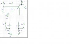
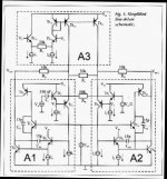
Certainly! See attached...
The top circuit is what I'm referring to as a fully differential input stage followed by a fully differential VAS stage, while the bottom circuit is what I'm calling a "pseudo differential" VAS stage, because the two VAS transistors (Q9 and Q7) do not share a common tail supply current source.
Also, to CBS240:
==> I built(building) an amp such as described, but using a common mode feedback.
Yes! This is the main point of what I'm trying to experiment with in my simulation - a method of common mode feedback so that the DC bias points of all points in the circuit are well defined. I can find many references on CMFB for IC opamp designs (opamps that are powered by less than 5V), but I can't find anything on CMFB methods for high voltage, high power fully differential amplifiers (such as an FD audio amplifier). May I ask, how did you implement your CMFB?
Ultimately, I would like to successfully simulate this kind of circuit (FD means fully differential for my shorthand notation):
An FD input stage with a current mirror tail source (for high CMRR) and an active load for each leg of the diff pair (this active load would also be made with a current mirror)
This would be followed by an FD VAS stage that also has a tail current source and an active load for each VAS transistor. To date, as I simulate the circuits in TopSpice with my methods of CMFB, my DC bias points are terrible....
Attachments
Thanks, Rtarbell, for your schematics. This is a very interesting discussion for me. I've sometimes seen a curious pseudo-differential stage loaded by a current mirror. The first fully differential stage I saw was the voltage stage of the JBL SA660 amplifier (1968, I think).
Hi CBS240,
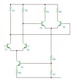
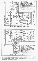
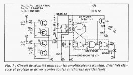
I have been thinking for long of the same idea as yours It has been used in some Kaneda regulated power supplies.
The attached image is the basic schematics in an all NPN configuration. It can't be used with a split power supply (+/gnd/-) for an outpout voltage at 0V. To achieve this, it needs additionnal circuit to refer the input voltages of the second stage to the negative power supply. An intermediate common base PNP stage with base voltage refered to the positive power supply could do it. Maybe you have some other ideas to implement a common mode loop, so my question is the same as Rtarbell : May I ask, how did you implement your CMFB?
Hi CBS240,
I have been thinking for long of the same idea as yours It has been used in some Kaneda regulated power supplies.
The attached image is the basic schematics in an all NPN configuration. It can't be used with a split power supply (+/gnd/-) for an outpout voltage at 0V. To achieve this, it needs additionnal circuit to refer the input voltages of the second stage to the negative power supply. An intermediate common base PNP stage with base voltage refered to the positive power supply could do it. Maybe you have some other ideas to implement a common mode loop, so my question is the same as Rtarbell : May I ask, how did you implement your CMFB?
Attachments
forr said:May I ask, how did you implement your CMFB?
Certainly
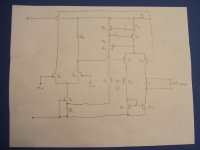
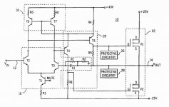
Here is a simplified drawing of what I’ve done. By simplified I mean my circuit uses cascode input stage and VAS, along with a more complex mirror for Q’s 11 & 12. I prefer J-fet inputs but I guess BJT would work also. I’m using very low current J-fets in an attempt to increase or eliminate R2 and R5. This means the input stage will be biased with just the base currents of the next stage, something around 10uA. In the last proto, the input stage bias is around 25uA.
You might be able to use a 2 transistor BJT CCS for Q1, but self bias J-fet here is simpler.🙂 R3 is chosen based upon the Pch J-fet’s Vgs @ Id for the correct current through R1. I used http://www.fairchildsemi.com/ds/MM/MMBF5460.pdf for Q6, but I suppose it doesn’t matter. Since a J-fet has no gate current, the gate can be used to sense the voltage on the CCS, Q4 & Q5 without affecting the CCS. When too much current tries to bias Q7, Q8 too heavily, the J-fet increases in conductance increasing voltage on R1 so current in Q1, and Q2/Q3 are reduced and bias less to Q7 & Q8, CMFB.🙂 The cascode Q9 is because most small J-fets don’t like lots of volts. VAS bias is set by 0.6V/R4. The active bias makes the circuit temperature independent because we all know that when electrons flow through a transistor it creates heat and the temperature rise increases gain and reduces Vbe, and affects bias. I’m sure there are other ways to implement some type of CMFB, but this seems to work for me. Simulation results might be interesting, I haven’t a good simulator so I just made a real circuit.😀
PS: I remembered that I made a thread about it a while ago. Not much discussion on CMFB though. The compensation isn't quite correct here but is too much hassle to change since there is a new circuit in the works, with some minor circuit changes, but more towards transistor arrays instead of completly descrete. Less component packages and better transistor matching with an actual PCB instead of veroboard.😀 That POS still works and sounds great though, believe it or not.:xeye
http://www.diyaudio.com/forums/showthread.php?threadid=90847&highlight=
Attachments
Thanks, CBS240, for publishing your very original schematics. CMFB is not a concept often seen implemented in power amplifiers, I like this way of stabilising the operating points.
Hi
One good thing about this circuit is DC offset is low, at least in the circuit I built. It depends on how well you match the devices, but IMO not needing a DC offset pot is beneficial. The proto-topology check circuit has about 15 mVDC with an Av of 65. In the new PCB(still only in existence on my computer🙄 ) there is a place for the R2 & R5, but I would like to not use them and bias just base current through the input LTP legs. I left options like this in the PCB so as different compensation techniques can be experimented with. The circuit in the link uses both Miller compensation and Miller feedback. Would like to try a 2 pole scheme. I am still doing some final clean-up work on the PCB though. I always hate the anxiety when ordering boards.

One good thing about this circuit is DC offset is low, at least in the circuit I built. It depends on how well you match the devices, but IMO not needing a DC offset pot is beneficial. The proto-topology check circuit has about 15 mVDC with an Av of 65. In the new PCB(still only in existence on my computer🙄 ) there is a place for the R2 & R5, but I would like to not use them and bias just base current through the input LTP legs. I left options like this in the PCB so as different compensation techniques can be experimented with. The circuit in the link uses both Miller compensation and Miller feedback. Would like to try a 2 pole scheme. I am still doing some final clean-up work on the PCB though. I always hate the anxiety when ordering boards.
Hi CBS240,
CMFB applied to the differential input of an audio amp is not a subject much covered. I wonder if there were other advantages than stable DC operating points. For example, cascoded input differential stages with upper pair bias referenced to the emitters of the input pair are known to have a good common mode rejection. I wonder if CMFB does the same job, or even better.
I have once seen the circuit shown here
http://www.diyaudio.com/forums/showthread.php?postid=1214396#post1214396
with some explanations in an american book about analog circuits , but I have never been able to find it again. Has anyone an idea of what book it could be ?
Hi forr
I once suggested in another thread using common mode feedback as a possible way to improve common mode rejection but was put off so I dropped the discussion. I don't think the implementation was understood though. It seems to me that if there were any changes in total current in the VAS diff at any time due to poor CMR, the CMFB would correct it by keeping both common mode currents proportionally equal, with respect to Hfe of VAS. This may also keep the VAS transistors from saturating during clipping as the limit is the current set by .6V/R4. Saturated transistors are slower to change leading to bad CMR. I will know more once the next circuit is made, but may take a few weeks. I'm no expert in audio, just a hobbyist. Of course the experts are always welcome to comment...
I think the thread starter may have lost interest.

rtarbell have you had a chance to simulate? I would be interested in comparing to some other more common circuit topologies, pros and cons.
I once suggested in another thread using common mode feedback as a possible way to improve common mode rejection but was put off so I dropped the discussion.
I don't think the implementation was understood though. It seems to me that if there were any changes in total current in the VAS diff at any time due to poor CMR, the CMFB would correct it by keeping both common mode currents proportionally equal, with respect to Hfe of VAS. This may also keep the VAS transistors from saturating during clipping as the limit is the current set by .6V/R4. Saturated transistors are slower to change leading to bad CMR. I will know more once the next circuit is made, but may take a few weeks. I'm no expert in audio, just a hobbyist. Of course the experts are always welcome to comment...I think the thread starter may have lost interest.
rtarbell have you had a chance to simulate? I would be interested in comparing to some other more common circuit topologies, pros and cons.
Hi lumanauw
I think that circuit would work well at DC if the devices are matched very closely, the CMFB active devices is the mirror not the input pair CCS. But wouldn't the gain of the input and VAS transistors be affected by the feedback loop😕 If one side increases current and the other does not decrease proportionally(creating a common mode output), then the feedback acts on both legs equally making it harder to keep balance in the input pair with reference to VAS tail current. If the tail current of the input diff is actively biased instead of each leg, then it can balance without any influence to either leg(or each VAS input) via a common mode input. I think the common mode input for the correction of a common mode error is important to always having balance in the input pair, which IMO is a must. I have not tried this circuit, just a first glance look. It would be interesting if someone with good simulator could try it and see how it works.
Forr
I wonder if that circuit in post 12 could be re-built to be better than say a 723 or similar regulator IC, maybe using some J-fets? It would be easier to create positive and negative regulators this way. For comparison, the simplified schem of a 723...
Attachments

Hi CBS240,
I am very familiar with the 723 which was wonderfully conceived some 40 years ago, I recently built a new lab power supply with it.
I think the Kaneda circuits are faster. Note that the voltage gain stage is entirely powered from the regulated side, in a somewhat incestuous manner, Ian Hickman should have said. I have no data at all on its performances. I would like to try a rather similar circuit in an amplifier.
May I explain why I am interested by this topology.
Cascading two devices of same polarity has been used for long in tubes and at the beginning of transistors. Then became the other polarity which made many things simpler. I once bought a vintage tuner and found immediately in love with its sound in the bass region. Fourteen years later, this love hasn't changed. As a transistor failed, I had to draw the circuit and I discovered that the output stage was a cascade of two NPN with the input bias is obtained from the emitter of the second transistor, then the whole is somewhat DC regulated. I thought that this circuit maybe more advantageuous from an audio point of view than a cascade of two devices of opposite polarity where currents increase or decrease in both devices at the same time. I already knew the Kaneda regulator with its double differential stage and I thought it had some familiarity with the simple twin NPN circuit and also, with some tube amp voltage stages. I recently learned that, in the Kaneda regulator, the feedback through the current source of the first stage is CMFB. I now enjoy that the idea of CMFB could lead to new audio amplifying circuits.
My simulator is currently Tina demo and I recently made my first steps with Microcap demo. I would like to have time to make some simulations of CMFB circuits.
Hi Lumanaw,
Its name itself implies that CMFB is hoped to reduce Common Mode Rejection. I have no data to submit.
The Kaneda schematics are all based on similar schemes :
Preamp
http://perso.orange.fr/audiotechno/html/realisations.htm
Amp, fig #8
http://www.tcaas.btinternet.co.uk/
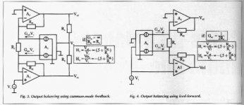
Having received so little returns about the subject of Common Mode Feedback puzzles me. I wonder if the concept is not that much known or if there is some kind of drawback when if used inside an amplifying circuit (someone should have told us). I have made some investigations and found this EDN article :
http://www.highbeam.com/doc/1G1-67326894.html
which can help to understand what is CMFB.
I then dig out an article written by Win de Jager from my Electronics World collection. It presents a parent concept of CMFB, even less known, the Common Mode FeedForward. I am all in favour of feedback but analysing this circuit could inspire some new ideas.
First, the general concepts of CMFB and CMFF
Attachments
- Status
- Not open for further replies.
- Home
- Amplifiers
- Solid State
- Fully differential and pseudo-differential stages